Display substrate and manufacturing method thereof and display device

A technology for a display substrate and a manufacturing method, which is applied to electrical components, electrical solid-state devices, circuits, etc., can solve the problems that affect the display quality of the display substrate, the film layer difference of the display substrate is large, and the anode is difficult to connect to the drain. Optimize the connection state, reduce the film layer difference, and improve the effect of the overlapping situation

Pending Publication Date: 2020-02-14
BOE TECH GRP CO LTD +1
View PDF8 Cites 4 Cited by
  • Summary
  • Abstract
  • Description
  • Claims
  • Application Information

AI Technical Summary

Problems solved by technology

[0002] In the OLED display substrate, the anode is connected to the drain of the thin film transistor through the via hole that runs through the flat layer. Due to the influence of the patterning process of the display substrate, the film layers in different regions of the display substrate have a large step difference, and a thicker flat layer is required. The display substrate is planarized, so that the depth of the via hole penetrating the flat layer is relatively large, which makes it difficult for the anode to overlap the drain electrode at the via hole, and poor lap bonding is likely to occur, which affects the display quality of the display substrate

Method used


Image

  • Display substrate and manufacturing method thereof and display device
  • Display substrate and manufacturing method thereof and display device
  • Display substrate and manufacturing method thereof and display device

Examples


Embodiment Construction

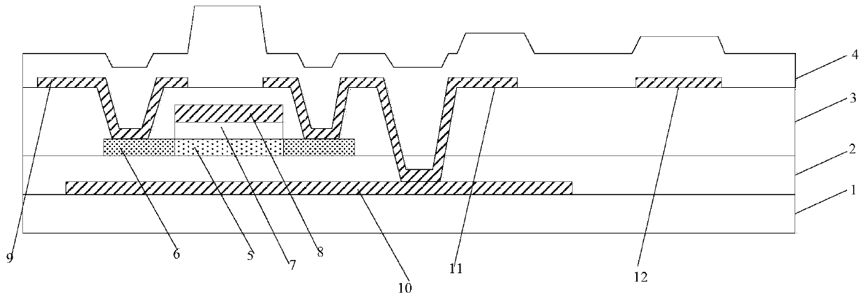
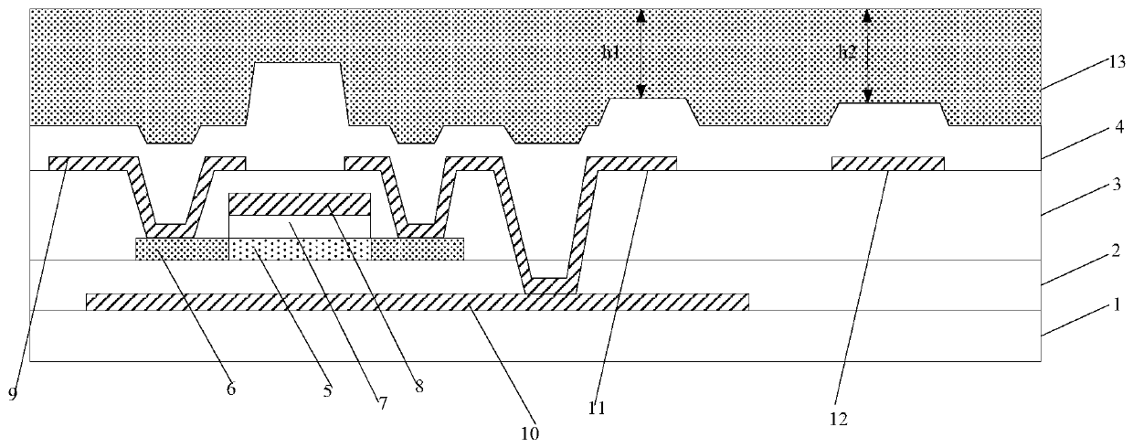
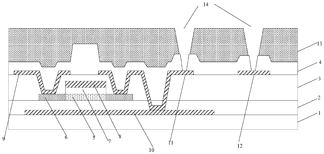
[0052] In order to make the technical problems, technical solutions and advantages to be solved by the embodiments of the present invention clearer, the following will describe in detail with reference to the drawings and specific embodiments.

[0053] The top-gate TFT (thin film transistor) has the characteristics of a short channel, so its on-state current Ion can be effectively increased, and when it is applied to a display substrate, it can significantly improve the display effect of the display substrate and effectively reduce the power consumption of the display substrate. Moreover, the overlapping area of ​​the gate and the source and drain of the top-gate TFT is small, so the parasitic capacitance generated is small, so the possibility of defects such as GDS (gate and source-drain short circuit) is also reduced. Since the top-gate TFT has the above-mentioned remarkable advantages, it has attracted more and more attention.

[0054] In recent years, due to the advantages...


PUM


Abstract

The invention provides a display substrate and a manufacturing method thereof and a display device, and belongs to the technical field of display. The display substrate comprises an underlayment substrate, a driving circuit layer located on the underlayment substrate, a flat layer covering the driving circuit layer, and a display electrode positioned on the flat layer. The display electrode is inlap joint with an output electrode of the driving circuit layer through a via hole penetrating through the flat layer. The output electrode comprises a first part in contact with the display electrodeand a second part except the first part. The display substrate further comprises a spacer structure located between the underlayment substrate and the first part, and the orthographic projection of the first part on the underlayment substrate is located in the orthographic projection of the spacer structure on the underlayment substrate. According to the technical scheme, the lap joint conditionof the display electrode and the output electrode can be improved, and the yield of the display substrate can be increased.

Description

technical field [0001] The present invention relates to the field of display technology, in particular to a display substrate, a manufacturing method thereof, and a display device. Background technique [0002] In the OLED display substrate, the anode is connected to the drain of the thin film transistor through the via hole that runs through the flat layer. Due to the influence of the patterning process of the display substrate, the film layers in different regions of the display substrate have a large step difference, and a thicker flat layer is required. The display substrate is planarized, so that the depth of the via hole penetrating the flat layer is relatively large, which makes it difficult for the anode to overlap with the drain electrode at the via hole, and poor bonding is prone to occur, thereby affecting the display quality of the display substrate. Contents of the invention [0003] The technical problem to be solved by the present invention is to provide a d...

Claims


Application Information

Patent Timeline
Patent Type & Authority Applications(China)
IPC IPC(8): H01L27/32
CPCH10K59/123H10K59/12H10K59/1213H10K59/1201
Inventor 刘宁刘军宋威程磊磊李伟李广耀
Owner BOE TECH GRP CO LTD
Why Eureka
Try Eureka