Reverse polarity vertical light emitting diode and its preparation method

A light-emitting diode and reverse polarity technology, which is applied in semiconductor devices, electrical components, circuits, etc., can solve the problems of carrier leakage efficiency, radiation efficiency drop, quantum well band bending, etc., and achieve good current expansion and active area The effect of large area and increased hole concentration

Active Publication Date: 2021-08-17
INST OF SEMICONDUCTORS - CHINESE ACAD OF SCI
View PDF11 Cites 0 Cited by
  • Summary
  • Abstract
  • Description
  • Claims
  • Application Information

AI Technical Summary

Problems solved by technology

At this time, the direction of the polarization electric field in the quantum well in the active region is the same as that of the applied forward working voltage, which will cause the energy band of the quantum well to bend (quantum confinement Stark effect), and the electrons and holes will wave in space. Function separation, radiative efficiency drops; causing carrier leakage and the resulting efficiency drop effect

Method used


Image

  • Reverse polarity vertical light emitting diode and its preparation method
  • Reverse polarity vertical light emitting diode and its preparation method
  • Reverse polarity vertical light emitting diode and its preparation method

Examples


preparation example Construction

[0060] The invention also discloses a method for preparing a reverse polarity vertical light-emitting diode, which includes the following steps:

[0061] Provide a temporary substrate on which a sacrificial layer, a p-type GaN-based semiconductor layer, a light-emitting layer and an n-type GaN-based semiconductor layer are sequentially deposited, and each layer exhibits metal polarity along the growth direction;

[0062] preparing an n-type electrode on the n-type GaN-based semiconductor layer;

[0063] providing a substrate, and bonding it to the above-mentioned n-type electrode;

[0064] remove the temporary substrate;

[0065] removing the remaining sacrificial layer to expose the p-type GaN-based semiconductor layer;

[0066] A p-type electrode is prepared on the p-type GaN-based semiconductor layer.

[0067] Wherein, the temporary substrate is selected from sapphire, silicon, silicon carbide, aluminum nitride, gallium nitride, gallium oxide, amorphous substrate or meta...

Embodiment 1

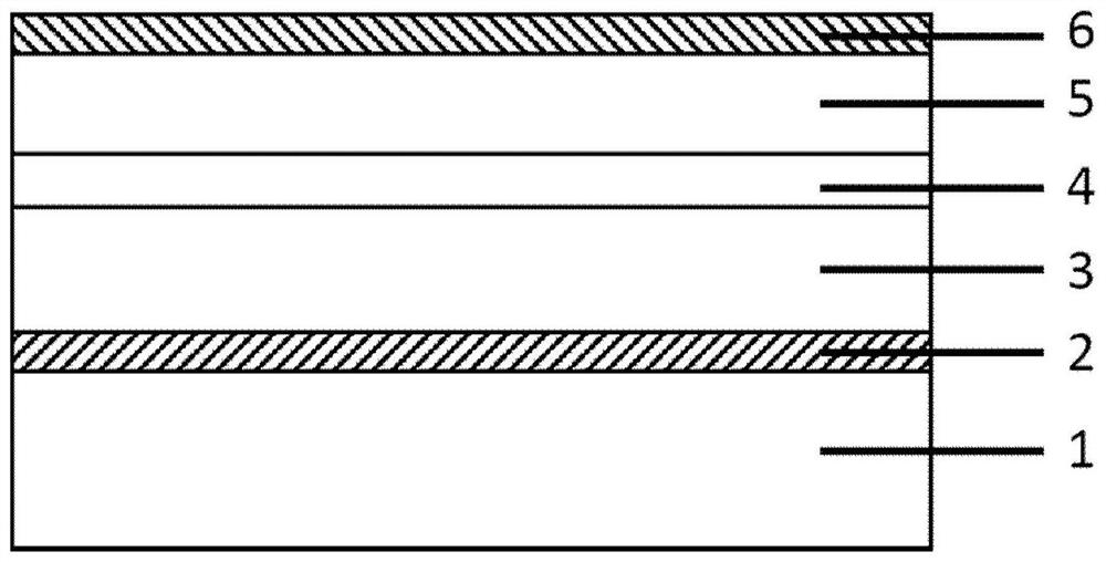
[0083] see figure 1 , the present invention provides a reverse polarity vertical light-emitting LED, including from bottom to top:

[0084] Substrate 1: its material can be silicon, ceramics, sapphire, silicon carbide, diamond, glass, metal or a combination thereof.

[0085] N-type electrode 2 : located on the substrate 1 . It can be a metal electrode with high reflectivity (such as Ag-based metal, Al-based metal, etc.), a transparent metal oxide electrode (such as indium tin oxide, magnesium oxide, magnesium zinc oxide, etc.) or a combination thereof. The n-type electrode 2 plays two roles, one is to form an ohmic contact with the semiconductor layer to realize electrical injection, and the other is to act as a reflector to emit back the photons transmitted to the side of the substrate 1, thereby increasing the escape probability of photons inside the LED .

[0086] N-type GaN-based semiconductor layer 3: located on the n-type electrode 2, it exhibits nitrogen polarity in ...

Embodiment 2

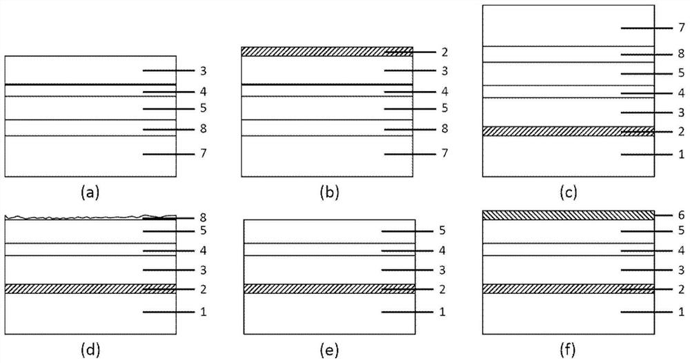
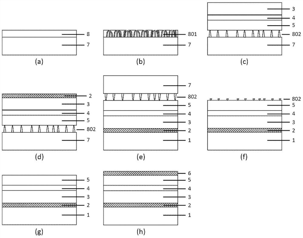
[0092] see figure 2 (a)-(f), the present invention provides a kind of preparation method of reverse polarity vertical light-emitting LED, and concrete steps comprise:

[0093] (1) A temporary substrate 7 is provided, on which a sacrificial layer 8 , a p-type GaN-based semiconductor layer 5 , a light-emitting layer 4 and an n-type GaN-based semiconductor layer 3 are sequentially deposited, and each layer exhibits metal polarity along the growth direction. The temporary substrate can be sapphire, silicon, silicon carbide, aluminum nitride, gallium nitride, gallium oxide, amorphous substrate or metal.

[0094] (2) The n-type electrode 2 is prepared on the n-type GaN-based semiconductor layer 3 . It can be a metal electrode with high reflectivity (such as Ag-based metal, Al-based metal, etc.), a transparent metal oxide electrode (such as indium tin oxide, magnesium oxide, magnesium zinc oxide, etc.) or a combination thereof.

[0095] (3) The substrate 1 is provided, and it is a...


PUM

PropertyMeasurementUnit
pore sizeaaaaaaaaaa
porosityaaaaaaaaaa

Abstract

A reverse polarity vertical light emitting diode and its preparation method, the reverse polarity vertical light emitting diode comprises: a substrate; an n-type electrode located on the substrate; an n-type GaN-based semiconductor layer located on the n-type electrode the light-emitting layer is located on the n-type GaN-based semiconductor layer; the p-type GaN-based semiconductor layer is located on the light-emitting layer; the p-type electrode is located on the p-type GaN-based semiconductor layer; The n-type GaN-based semiconductor layer, light-emitting layer and p-type GaN-based semiconductor layer all show nitrogen polarity in the bottom-up direction, and show metal polarity in the top-down direction. The present invention integrates the advantages of reverse polarity and vertical structure, can effectively increase the hole concentration of the p-type GaN-based semiconductor layer, suppress the quantum-confined Stark effect in the active region of the quantum well, thereby improving the radiation recombination efficiency and internal quantum of the LED Efficiency, improving the luminous performance and reliability of LEDs.

Description

technical field [0001] The invention relates to the technical field of light emitting diodes, in particular to a reverse polarity vertical light emitting diode and a preparation method thereof. Background technique [0002] Since the 1990s, GaN-based light-emitting diodes (Light-emitting diodes, LEDs) have attracted widespread attention and achieved rapid development. GaN-based LEDs have significant advantages such as adjustable wavelength, light and flexible, low energy consumption, low working voltage, directional light emission, no pollution, long life, and fast response time. Curing, sterilization and disinfection have huge market value. [0003] GaN-based materials with a wurtzite structure lack central inversion symmetry in the c-axis direction, and the positive and negative charging centers of the unit cell do not coincide, and the material exhibits polarity under macroscopic conditions. Generally, the GaN-based material grown on the low-temperature buffer layer by ...

Claims


Application Information

Patent Timeline
Patent Type & Authority Patents(China)
IPC IPC(8): H01L33/32H01L33/20H01L33/06H01L33/00
CPCH01L33/0075H01L33/06H01L33/20H01L33/32
Inventor 郭亚楠闫建昌王军喜李晋闽
Owner INST OF SEMICONDUCTORS - CHINESE ACAD OF SCI
Why Eureka
Try Eureka