An epitaxy method to improve current spreading of gan-based LED chips

A LED chip and current expansion technology, which is applied to circuits, electrical components, semiconductor devices, etc., can solve problems such as voltage increase and chip leakage increase, and achieve the effects of improving uniformity, reducing local junction temperature, and overcoming brightness aggregation phenomenon

Active Publication Date: 2017-10-13
宁波安芯美半导体有限公司
View PDF4 Cites 0 Cited by
  • Summary
  • Abstract
  • Description
  • Claims
  • Application Information

AI Technical Summary

Problems solved by technology

Generally, the resistance can be reduced by increasing the amount of Si doping in the GaN layer, and the resistance can be increased by reducing the amount of Si doping, but this method often leads to undesirable electrical losses such as increased chip leakage and increased voltage.

Method used


Image

  • An epitaxy method to improve current spreading of gan-based LED chips
  • An epitaxy method to improve current spreading of gan-based LED chips
  • An epitaxy method to improve current spreading of gan-based LED chips

Examples


Embodiment 1

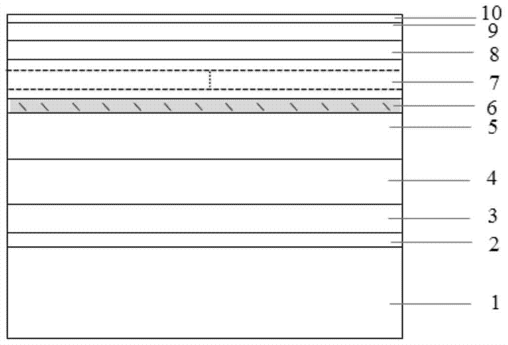
[0033] An epitaxial method for improving the current expansion of a GaN-based LED chip, the method comprising the following specific steps:

[0034] Step 1, annealing the sapphire substrate 1 in a hydrogen atmosphere, cleaning the surface of the sapphire substrate 1, controlling the temperature at 1040° C., and then performing nitriding treatment for 5 minutes;

[0035] Step 2: Lower the temperature to 500°C, grow a 20nm-thick low-temperature GaN nucleation layer 2, control the growth pressure at 450Torr, set the V / III molar ratio at 60, and use TMGa as the Ga source;

[0036] Step 3: After the growth of the low-temperature GaN nucleation layer 2 is completed, stop feeding TMGa, perform in-situ annealing treatment, the annealing temperature is 1020°C, and the annealing time is 5 minutes; after annealing, adjust the temperature to 980°C, and the epitaxial growth thickness is 600nm High-temperature GaN buffer layer 3, the growth pressure is 450 Torr, the V / III molar ratio is 200...

Embodiment 2

[0048] An epitaxial method for improving the current expansion of a GaN-based LED chip, the method comprising the following specific steps:

[0049] Step 1, annealing the sapphire substrate 1 in a hydrogen atmosphere, cleaning the surface of the sapphire substrate 1, controlling the temperature at 1080°C, and then performing nitriding treatment for 10 minutes;

[0050] Step 2: Lower the temperature to 550°C, grow a 40nm-thick low-temperature GaN nucleation layer 2, control the growth pressure at 550Torr, keep the V / III molar ratio at 120, and use TMGa as the Ga source;

[0051] Step 3: After the growth of the low-temperature GaN nucleation layer 2 is completed, stop feeding TMGa, perform in-situ annealing treatment, the annealing temperature is 1050°C, and the annealing time is 10 minutes; after the annealing, adjust the temperature to 1050°C, and the epitaxial growth thickness is 800nm High-temperature GaN buffer layer 3, the growth pressure is 550 Torr, the V / III molar ratio...


PUM

PropertyMeasurementUnit
thicknessaaaaaaaaaa
thicknessaaaaaaaaaa
thicknessaaaaaaaaaa

Abstract

The invention provides an epitaxial method for improving GaN based LED chip current spreading. An epitaxial structure comprises a sapphire substrate, a low-temperature GaN nucleating layer, a high-temperature GaN buffer layer, a high-temperature u-type GaN layer, a composite n-type GaN layer, a composite current spreading layer, a multi-quantum well light-emitting layer, a p-type AlGaN electron blocking layer, a high-temperature p-type GaN layer and a p-type GaN contact layer from bottom to top in sequence. After the composite n-type GaN layer finishes growing, the composite current spreading layer grows; the composite current spreading layer is composed of 15-20 groups of u-GaN / n-GaN superlattices and 5-10 groups of n-GaN / n-AlGaN superlattices. Current spreading of a prolate chip can be improved remarkably, local junction temperature of the chip is lowered, uniformity of light-emitting brightness distribution of the chip is improved, and the whole chip is uniform in light emission without brightness gathering.

Description

technical field [0001] The invention relates to the technical field of GaN-based LED preparation, in particular to an epitaxy method for improving the current expansion of a GaN-based LED chip. Background technique [0002] Semiconductor light-emitting diodes (light-emission diodes, LEDS) have shown irreplaceable advantages in the field of backlight applications due to their small size, low energy consumption, long life, environmental protection and durability. With the continuous upgrading of backlight application products such as mobile phones and liquid crystal displays, the requirements for LED chips for backlight are also getting higher and higher. At present, the backlight chips are gradually developing in the direction of oblong shape, but according to experience, once the aspect ratio of the chip exceeds 4, because the electrodes are designed at both ends of the long side of the chip, there will be uneven current expansion, resulting in local junction temperature of ...

Claims


Application Information

Patent Timeline
Patent Type & Authority Patents(China)
IPC IPC(8): H01L33/00H01L33/32
CPCH01L33/007H01L33/06H01L33/145H01L33/32
Inventor 唐军
Owner 宁波安芯美半导体有限公司
Why Eureka
Try Eureka