GaN high-efficiency light-emitting diode based on physical polishing roughening ITO layer and manufacturing method

A light-emitting diode, grinding and roughening technology, applied in the field of microelectronics, can solve the problems of long period of light-emitting diodes, high cost, complex process, etc., and achieve the effects of improving light extraction efficiency, reducing costs, and simplifying the process

Inactive Publication Date: 2019-03-29
XIDIAN UNIV
View PDF2 Cites 0 Cited by
  • Summary
  • Abstract
  • Description
  • Claims
  • Application Information

AI Technical Summary

Problems solved by technology

[0005] At present, there are many common ways to roughen the surface of the ITO layer, such as nanoimprinting to form air cavities, stripe etching, etc. Although the effect of these methods is relatively improved, the production process is very complicated, which leads to the production of luminous Diodes have long cycle times and high costs

Method used


Image

  • GaN high-efficiency light-emitting diode based on physical polishing roughening ITO layer and manufacturing method
  • GaN high-efficiency light-emitting diode based on physical polishing roughening ITO layer and manufacturing method

Examples


Embodiment 1

[0037] Example 1, preparing a light emitting diode with a light emission wavelength of 370nm.

[0038] In step one, the substrate is pretreated.

[0039] After the sapphire substrate was cleaned, it was placed in the metal organic chemical vapor deposition MOCVD reaction chamber, and the vacuum degree of the reaction chamber was reduced to 2×10 -2 Torr: Introduce the mixed gas of hydrogen and ammonia into the reaction chamber, and under the condition that the pressure of the MOCVD reaction chamber reaches 20 Torr, the substrate is heated to a temperature of 750°C and kept for 10 minutes to complete the pretreatment of the substrate.

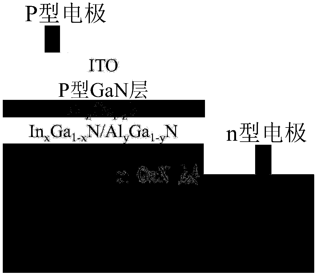
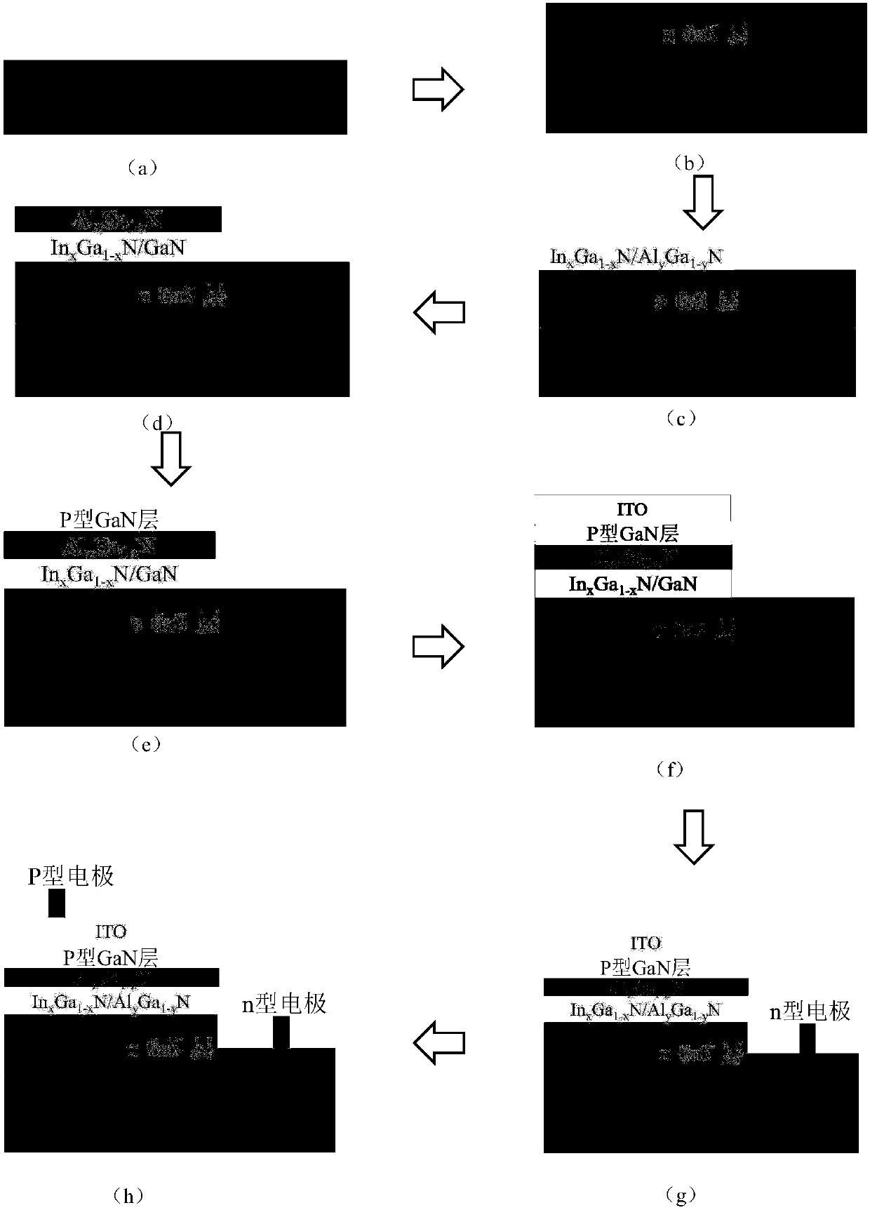
[0040] Step 2, using the MOCVD process to grow a high-temperature AlN layer, such as figure 2 (a).

[0041] Adjust the temperature of the reaction chamber to 950°C, feed ammonia gas with a flow rate of 2500 sccm and an aluminum source with a flow rate of 40 sccm at the same time, and grow a high-temperature AlN substrate with a thickness of 50 n...

Embodiment 2

[0061] Example 2, preparing a light emitting diode with a light emitting wavelength of 410 nm.

[0062] Step 1, pretreating the substrate.

[0063] After the sapphire substrate was cleaned, it was placed in the metal organic chemical vapor deposition MOCVD reaction chamber, and the vacuum degree of the reaction chamber was reduced to 2×10 -2 Torr: Introduce the mixed gas of hydrogen and ammonia into the reaction chamber, and under the condition that the pressure of the MOCVD reaction chamber reaches 780 Torr, the substrate is heated to a temperature of 1000°C and kept for 5 minutes to complete the pretreatment of the substrate

[0064] Step 2, using the MOCVD process to grow a high-temperature AlN layer, such as figure 2 (a).

[0065] The temperature of the reaction chamber was adjusted to 900°C, and the ammonia gas with a flow rate of 2000 sccm and the aluminum source with a flow rate of 20 sccm were fed at the same time, and the pressure was maintained at 60 Torr to grow ...

Embodiment 3

[0084] Example 3, preparing a light emitting diode with a light emitting wavelength of 540nm.

[0085] Step A, pretreating the substrate.

[0086] After the c-plane sapphire substrate was cleaned, it was placed in the metal organic chemical vapor deposition MOCVD reaction chamber, and the vacuum degree of the reaction chamber was reduced to 2×10 -2 Torr: Introduce the mixed gas of hydrogen and ammonia into the reaction chamber, and under the condition that the pressure of the MOCVD reaction chamber reaches 120 Torr, the substrate is heated to a temperature of 850°C and kept for 8 minutes to complete the pretreatment of the substrate.

[0087] In step B, a high-temperature AlN layer is grown by MOCVD process.

[0088] Adjust the temperature of the reaction chamber to 1000°C, feed ammonia gas with a flow rate of 3000 sccm and an aluminum source with a flow rate of 30 sccm at the same time, and grow a high-temperature AlN substrate with a thickness of 110 nm on the nitrided subs...


PUM


Abstract

The invention discloses a GaN high-efficiency light-emitting diode based on a physical polishing roughening ITO layer and a manufacturing method, and mainly solves problems of complicated process andlow luminous efficiency of an existing ITO roughening process. The GaN high-efficiency light-emitting diode includes, from bottom to top: a sapphire substrate layer (1), a high-temperature AlN nucleation layer (2), a n-type GaN layer (3), an InxGa1-xN / GaN multiple quantum well layer (4), an AlzGa1-zN electron blocking layer (5), a p-type GaN layer (6), a polished roughened indium tin oxide ITO layer (7), and an electrode (8). The polishing roughening method uses diamond sandpaper to polish, and surface roughness after polishing and roughening is 10-100nm. An ITO layer roughening process is simplified, efficiency of a light-emitting diode is improved, and the light-emitting diode can be used for illumination, biology, medical treatment, anti-counterfeiting identification, purification and data storage.

Description

technical field [0001] The invention belongs to the technical field of microelectronics, and in particular relates to a high-efficiency light-emitting diode, which can be used in lighting, biology, medical treatment, anti-counterfeiting identification, purification and data storage. technical background [0002] Light-emitting diodes have become the mainstream lighting source of the next generation due to their low power consumption, long life, small size, and environmental protection. At present, the industrial demand for high-brightness light-emitting diodes is increasing rapidly, so it is very important to improve the luminous efficiency of light-emitting diodes. Under the same working conditions, higher luminous efficiency means higher luminous intensity; under the same luminous intensity, higher Excellent luminous efficiency means lower power consumption. [0003] The quality of internal current expansion of light-emitting diodes is one of the important factors affecti...

Claims


Application Information

Patent Timeline
Patent Type & Authority Applications(China)
IPC IPC(8): H01L33/14H01L33/22H01L33/00
Inventor 许晟瑞王学炜范晓萌郝跃张进成李培咸张春福马晓华毕臻周小伟
Owner XIDIAN UNIV
Why Eureka
Try Eureka