
A method for preparing patterned transparent conductive film by laser

A transparent conductive film and patterning technology, which is applied in the direction of equipment, circuits, and electrical components used to manufacture conductive/semiconductive layers, can solve the problems of limiting film light transmittance, lack of flexibility, etc., and achieve fast, High flexibility and high precision effect

Active Publication Date: 2021-08-24
WUHAN UNIV
View PDF9 Cites 0 Cited by
  • Summary
  • Abstract
  • Description
  • Claims
  • Application Information

AI Technical Summary

Problems solved by technology

[0004] In previous studies, the researchers prepared a nano-silver film with good conductivity, but because the silver nano-material is uniformly distributed in the film, the light transmittance of the film is limited; although the invention patent CN 104795130 A has published a A method for preparing a patterned transparent conductive film, but the patterned grooves are prepared by an embossing process, which lacks flexible and variable characteristics

Method used


Image

  • A method for preparing patterned transparent conductive film by laser
  • A method for preparing patterned transparent conductive film by laser
  • A method for preparing patterned transparent conductive film by laser

Examples


Embodiment 1

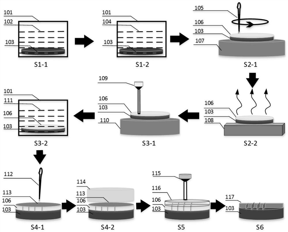
[0037] Such as figure 1 As shown, the method for preparing a patterned transparent conductive film by laser provided in the first embodiment specifically includes the following steps:

[0038] S1-1. Add 100ml of acetone solution 102 into a 500ml beaker 101, then clamp a 2-inch Sapphire substrate 103 into the beaker 101 with tweezers, and clean the organic impurities on the surface of the Sapphire substrate 103;

[0039] S1-2. Pour off the acetone solution 102, add absolute ethanol (99.7wt.%) 104, also clamp the Sapphire substrate 103 into the beaker with tweezers, and clean the remaining acetone solution 102 on the surface of the substrate;

[0040] S2-1. After cleaning and drying the substrate 103, place it on the spin coater 107, drop a few drops of photoresist on the substrate 103 with the first dropper 105, then turn on the spin coater 107 and start to rotate, set The rotation speed is 4000rpm, the rotation time is 30s, and the photoresist coating 106 is obtained; (the ph...

Embodiment 2

[0049] Such as figure 1As shown, the method for preparing a patterned transparent conductive film by laser provided in the first embodiment specifically includes the following steps:

[0050] S1-1. Add 100ml of acetone solution 102 into a 500ml beaker 101, then clamp a 2-inch Sapphire substrate 103 into the beaker 101 with tweezers, and clean the organic impurities on the surface of the Sapphire substrate 103;

[0051] S1-2. Pour off the acetone solution 102, add absolute ethanol (99.7wt.%) 104, also clamp the Sapphire substrate 103 into the beaker with tweezers, and clean the remaining acetone solution 102 on the surface of the substrate;

[0052] S2-1. After cleaning and drying the substrate 103, place it on the spin coater 107, drop a few drops of photoresist on the substrate 103 with the first dropper 105, then turn on the spin coater 107 and start to rotate, set The rotation speed is 6000rpm, the rotation time is 20s, and the photoresist coating 106 is obtained; (the pho...


PUM

PropertyMeasurementUnit
particle diameteraaaaaaaaaa

Abstract

The invention relates to a method for preparing a patterned transparent conductive film by laser, which comprises the following steps: 1) cleaning the substrate; 2) spin-coating a photoresist on the substrate and drying it; 3) designing a pattern using a laser direct writing device and covering it Exposing the patterned area on the substrate with photoresist, and then removing the photoresist corresponding to the patterned area with a developer; 4) coating the silver nano-slurry on the patterned area to occupy the area after removing the photoresist, and then Use the grinding method to ensure that the thickness of the silver nano-slurry and the remaining photoresist are uniform; 5) Press the light-transmitting sheet on the patterned area obtained in step 4), and then the laser passes through the light-transmitting sheet to scan the patterned area of ​​the substrate , sintering and curing the silver nano paste; 6) removing the remaining photoresist to obtain a patterned transparent conductive film. The method can design patterns arbitrarily, realizes the patterning of the transparent conductive film conveniently and quickly, and has strong flexibility and good repeatability.

Description

technical field [0001] The invention belongs to the field of photoelectric materials and technologies, and in particular relates to a method for preparing a patterned transparent conductive film by laser. Background technique [0002] Because of the scarcity of indium and the brittle ceramic properties of indium tin oxide (ITO), ITO, as a transparent conductive film, has affected the rapid development of electronic devices, such as wearable devices, photovoltaic devices, and AR fields. In recent years, research on new transparent conductive films to replace ITO has received extensive attention. [0003] Researchers have also tried some alternatives, such as graphene, carbon nanotubes and silver nanomaterials. Both graphene and carbon nanotubes belong to carbon-based nanomaterials. Because of the low intrinsic carrier concentration or the high resistance between layers, the films prepared by the two materials have high square resistance. . Silver nanomaterials belong to me...

Claims


Application Information

Patent Timeline
Patent Type & Authority Patents(China)
IPC IPC(8): H01B13/00
CPCH01B13/0026
Inventor 周圣军赵强桂成群万辉于圣韬
Owner WUHAN UNIV
Learn More