Vacuum sputtering mixed light-cured resin packaging process for organic electronic device

An organic electronic device, photocurable resin technology, applied in the direction of electric solid devices, electrical components, semiconductor devices, etc., can solve the problems of low packaging yield, multiple materials, poor durability and stability, etc., to improve the yield and packaging. performance, the effect of improving the overall effect

Pending Publication Date: 2020-02-25
FLEXIBLE JIANGSU MATERIALS CO LTD
View PDF4 Cites 1 Cited by
  • Summary
  • Abstract
  • Description
  • Claims
  • Application Information

AI Technical Summary

Problems solved by technology

[0012] The purpose of the present invention is to provide two packaging process designs and schemes that mix dense inorganic nanomaterials and organic photocurable materials into packaging layers, so as t

Method used


Image

  • Vacuum sputtering mixed light-cured resin packaging process for organic electronic device
  • Vacuum sputtering mixed light-cured resin packaging process for organic electronic device

Examples


Embodiment 1

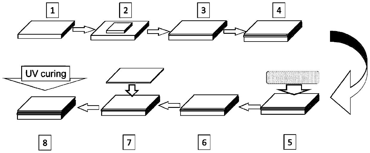
[0051] According to the design and process of the invention, the hybrid packaging structure and steps of vacuum sputtering and photocuring resin are as follows:

[0052] According to the design and process of the invention, its packaging scheme is very simple and practical, and the following steps are adopted:

[0053] In the first step, the ready glass or high-barrier flexible substrate is prepared, and the surface can be cleaned. And put it into a vacuum drying oven to remove more than adsorbed water vapor and oxygen. Putting glass or high-barrier flexible substrates into organic electronic device equipment completes the preparation of organic device OLEDs.

[0054] The third step is to prepare 100nm LiF on the prepared OLED device, or Al 2 o 3 Film protective layer.

[0055] The fourth step is to transfer the sample into a nitrogen glove box with water and oxygen less than 1ppm at 20°C. Apply a layer of UV curable resin by spin coating, hang coating process, about 5-50...

Embodiment 2

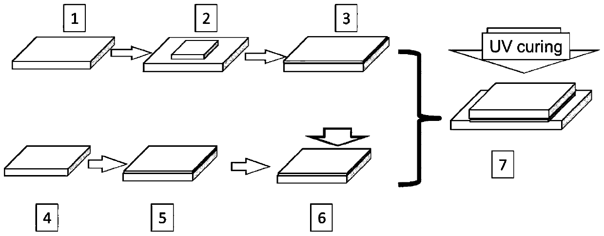
[0061] According to the design and process of the invention, the hybrid packaging structure and steps of vacuum sputtering and photocuring resin are as follows:

[0062] According to the design and process of the invention, its packaging scheme is very simple and practical, and the following steps are adopted:

[0063] In the first step, the ready glass or high-barrier flexible substrate is prepared, and the surface can be cleaned. And put it into a vacuum drying oven to remove more than adsorbed water vapor and oxygen. Putting glass or high-barrier flexible substrates into organic electronic device equipment completes the preparation of organic device OLEDs.

[0064] In the third step, 100nm LiF, Al 2 o 3 Film protective layer.

[0065] In the fourth step, at the same time as the first three steps, the upper packaging glass or film is introduced into a nitrogen glove box at 20°C, water, and oxygen less than 1ppm. Apply a layer of UV curable resin by spin coating, hang co...


PUM

PropertyMeasurementUnit
Thicknessaaaaaaaaaa

Abstract

The invention discloses a mixed packaging structure and process for two ultrathin flexible organic electronic devices. A preparation process of mixing nano sputtering and organic curing resin is mainly utilized, a compact nano material with a high packaging effect is semi-injected into an organic material resin layer, and then photocuring is carried out to greatly improve the water and oxygen blocking capability of organic cured resin in the packaging process, so that the packaging efficiency, the packaging yield and the reliability of UV cured gluing resin are greatly improved while the packaging and curing of organic devices are ensured. The process can be applied to high-performance water and oxygen blocking packaging of various ultrathin and flexible organic electronic devices, and particularly can combine a nano-film layer with an organic photocuring numerical value to realize efficient packaging of the ultrathin organic electronic devices.

Description

Technical field: [0001] The invention belongs to the technical field of packaging of organic electronic devices, and in particular relates to a vacuum sputtering mixed light-curing resin packaging process for organic electronic devices. Background technique: [0002] New organic electronic devices, organic light emitting devices, organic optoelectronic devices, organic detectors and organic field effect tubes are used in mobile phones, TVs and other displays and solid-state lighting, energy sources, detectors, Mobile phones have broad application prospects in the future wearable field. Its excellent optoelectronic properties will affect the development of next-generation display electronics, and will be the mainstay of ultra-thin and flexible electronic displays. [0003] However, according to a long-term, a large number of organic electronics studies have shown that water vapor and oxygen molecules in the air have a fatal impact on organic electronic devices, the main reas...

Claims


Application Information

Patent Timeline
IPC IPC(8): H01L51/40H01L51/48H01L51/56H01L51/10H01L51/44H01L51/52
CPCH10K71/00H10K10/88H10K30/88H10K50/844H10K50/84Y02E10/549
Inventor 林群
Owner FLEXIBLE JIANGSU MATERIALS CO LTD
Why Eureka
Try Eureka