Supercharge Your Innovation With Domain-Expert AI Agents!

Semi-subtractive high-precision etching method

A high-precision, subtractive technology, used in the removal of conductive materials by chemical/electrolytic methods, electrical components, printed circuit manufacturing, etc., can solve the problem that thin copper circuits cannot meet market demand, and achieves solutions to manufacturing difficulties and satisfaction. Electronic technology requirements, the effect of ensuring precision

Active Publication Date: 2020-02-28
江苏上达半导体有限公司
View PDF7 Cites 1 Cited by
  • Summary
  • Abstract
  • Description
  • Claims
  • Application Information

AI Technical Summary

Problems solved by technology

[0005] The purpose of the present invention is to provide a high-precision etching method with a half reduction method to solve the above-mentioned background technology, which is limited by the current exposure technology and etching technology, and can only make fine lines on thin copper foils, but due to electronic Products are becoming increasingly complex and diverse, and thin copper lines can no longer meet market demand

Method used


Image

  • Semi-subtractive high-precision etching method
  • Semi-subtractive high-precision etching method
  • Semi-subtractive high-precision etching method

Examples


Embodiment Construction

[0027] The technical solutions in the embodiments of the present invention will be clearly and completely described below in conjunction with the embodiments of the present invention. Apparently, the described embodiments are only some of the embodiments of the present invention, not all of them. Based on the embodiments of the present invention, all other embodiments obtained by persons of ordinary skill in the art without making creative efforts belong to the protection scope of the present invention.

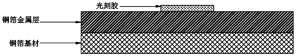
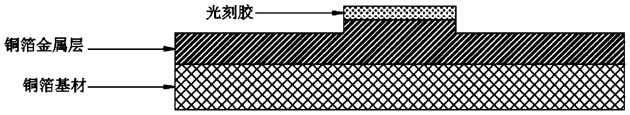
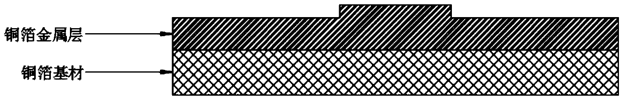
[0028] see Figure 1 to Figure 7 , in an embodiment of the present invention, a semi-subtractive high-precision etching method includes the following steps:

[0029] Sp1: Prepare the copper foil substrate, apply photoresist on the copper foil metal layer of the copper foil substrate, and perform exposure and development treatment;

[0030] Sp2: Etching the copper foil metal layer, the etching thickness range is 5um-10um, to ensure the fineness of etching;

[0031] Sp3: Stri...


PUM


Abstract

The invention discloses a semi-subtractive high-precision etching method and relates to the technical field of circuit processing. The method comprises steps that Sp1, a copper foil base material is prepared, photoresist is coated on a copper foil metal layer of the copper foil base material, and exposure and development treatment are performed; Sp2, a copper foil metal layer surface is subjectedto etching treatment, and the etching thickness ranges from 5 microns to 10 microns, so etching fineness is guaranteed; Sp3, stripping treatment of the redundant photoresist on the metal layer surfaceof the copper foil is performed; and Sp4, an impedance agent is coated or attached on the metal layer surface of the copper foil. The method is advantaged in that precision of a fine circuit manufactured by the method is determined by the first coating or exposure resolution of an attached material and has nothing to do with secondary coating or the attached material, thickness of the metal layeretched for the first time is 5-10 microns, so the mature thin copper etching technology is met, precision of the circuit can be ensured, manufacturing difficulty of a thick copper fine circuit is solved, fine circuits with different thicknesses can be produced, and the increasingly developed electronic technical requirements are met.

Description

technical field [0001] The invention relates to the technical field of circuit processing, in particular to a high-precision etching method using a semi-subtractive method. Background technique [0002] With the continuous development of electronic technology, electronic products are developing in the direction of light, thin, short, small, multi-functional and high reliability. Printed circuit boards have the characteristics of high wiring density, light weight, and good heat dissipation performance, which is in line with the current development trend of electronic products, so printed circuit boards are more and more widely used. However, electronic products are becoming increasingly complex and diverse, so new requirements are placed on the circuit design of printed circuit boards. Lines affect impedance, and how to ensure the integrity of various signals (especially high-speed signals) needs to be realized through line design. Line design includes line width, line spac...

Claims


Application Information

Patent Timeline
Patent Type & Authority Applications(China)
IPC IPC(8): H05K3/06
CPCH05K3/06H05K2203/1476
Inventor 杨媚莲王健杨洁孙彬沈洪李晓华
Owner 江苏上达半导体有限公司
Features
  • R&D
  • Intellectual Property
  • Life Sciences
  • Materials
  • Tech Scout
  • Unparalleled Data Quality
  • Higher Quality Content
  • 60% Fewer Hallucinations
Learn More