Wafer mapping production management method, device, system, medium and computer equipment

A technology of production equipment and production management, applied in the direction of database management system, calculation, multi-program device, etc., can solve the problem of low management convenience, achieve the effect of improving reliability, improving convenience, and convenient and reliable operation

Pending Publication Date: 2020-03-20
O FILM IMAGE TECH (GUANGZHOU) CO LTD
View PDF6 Cites 2 Cited by
  • Summary
  • Abstract
  • Description
  • Claims
  • Application Information

AI Technical Summary

Problems solved by technology

[0004] Based on this, it is necessary to address the technical problem of low management convenience in the traditional wafer mapping system, and provide a wafer mapping production management method, device, system, medium and computer equipment with high management convenience

Method used


Image

  • Wafer mapping production management method, device, system, medium and computer equipment
  • Wafer mapping production management method, device, system, medium and computer equipment
  • Wafer mapping production management method, device, system, medium and computer equipment

Examples


Embodiment Construction

[0048] In order to make the purpose, technical solutions, and advantages of this application clearer, the following further describes the application in detail with reference to the accompanying drawings and embodiments. It should be understood that the specific embodiments described here are only used to explain the application, and not used to limit the application.

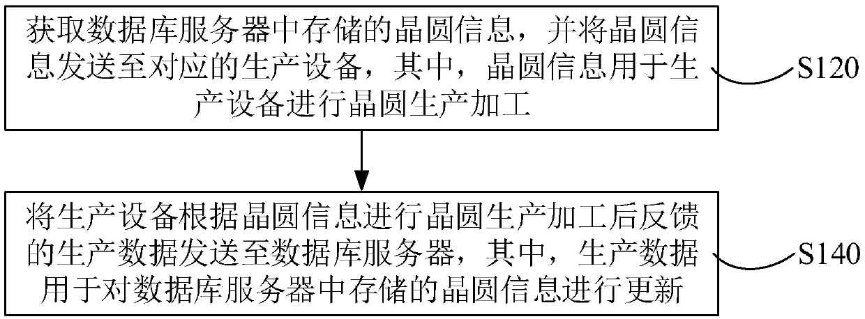
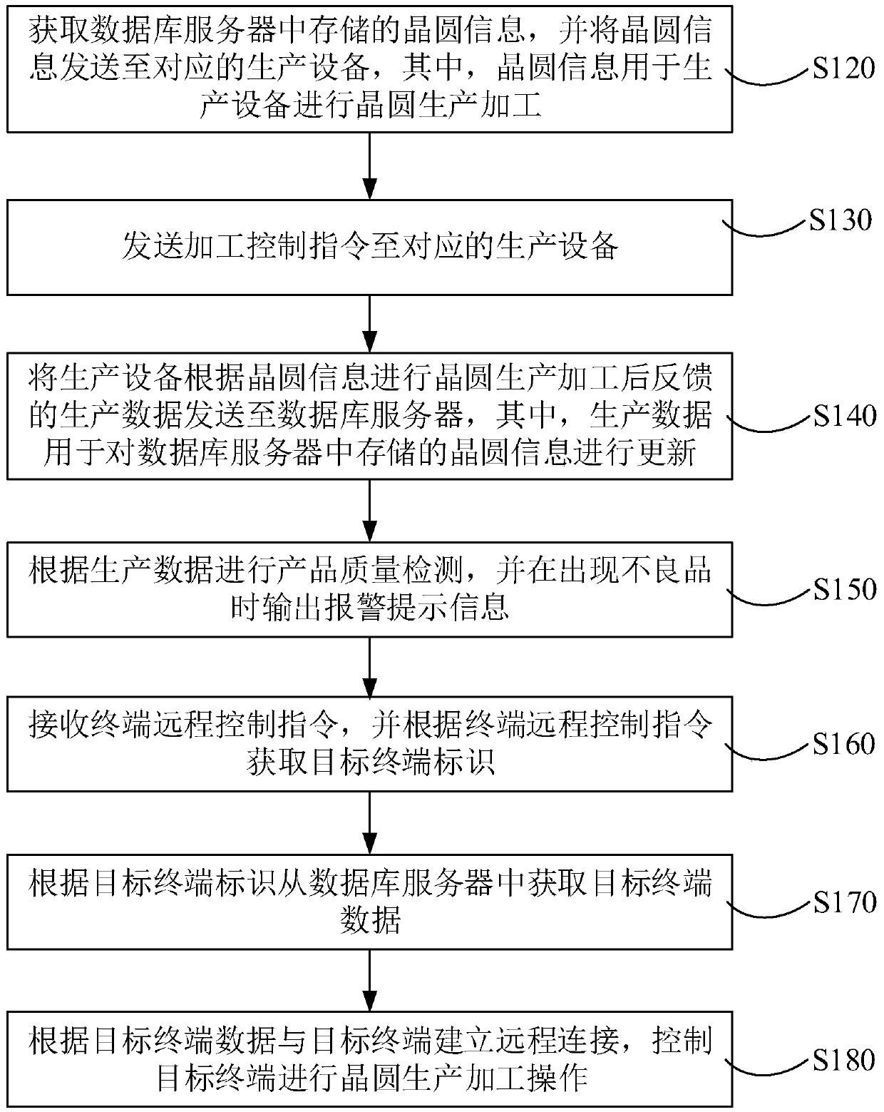
[0049] In one embodiment, a wafer mapping production management method is provided, such as figure 1 As shown, the method includes:

[0050] Step S120: Obtain the wafer information stored in the database server, and send the wafer information to the corresponding production equipment, where the wafer information is used by the production equipment for wafer production processing.

[0051] The wafer information is obtained from the database server through the terminal and forwarded to the corresponding production equipment. The terminal may specifically be a computer, mobile phone, notebook, etc. The number of termin...


PUM


Abstract

The invention relates to a wafer mapping production management method, a device, a system, a medium and computer equipment, and the method comprises the steps: obtaining wafer information stored in adatabase server, transmitting the wafer information to corresponding production equipment, and enabling the wafer information to serve as the production equipment for wafer production and processing;and sending production data fed back by the production equipment after wafer production and processing according to the wafer information to a database server for updating the wafer information storedin the database server to serve as data required by subsequent wafer processing. Through information interaction with the production equipment and the database server, feedback of production data andstorage and updating of wafer information are completed, workers can manage the wafer information, information collection is facilitated, and the management convenience of wafer mapping production isimproved.

Description

Technical field [0001] The present invention relates to the field of semiconductor processing technology, in particular to a wafer mapping production management method, device, system, medium and computer equipment. Background technique [0002] Semiconductor packaging refers to the process of processing the tested wafers according to the product model and functional requirements to obtain independent chips. Due to the continuous development of CPU (Central Processing Unit, central processing unit) and other very large integrated circuits, the packaging forms of integrated circuits are constantly adjusted and changed, and the progress of packaging forms will in turn promote the development of chip technology. [0003] At present, semiconductor packaging equipment such as Die Bond (die bond) equipment, Flip Chip (flip chip) equipment, etc. have built-in wafer mapping systems. The traditional wafer mapping system is integrated inside the equipment, and the system directly reads the ...

Claims


Application Information

Patent Timeline
Patent Type & Authority Applications(China)
IPC IPC(8): G06Q10/06G06F16/23G06F16/25G06Q50/04G06F9/54
CPCG06Q10/06G06F9/546G06F9/548G06Q50/04G06F2209/548G06F2209/544Y02P90/30
Inventor 文桂球
Owner O FILM IMAGE TECH (GUANGZHOU) CO LTD
Why Eureka
Try Eureka