Modeling method considering node voltage dynamic change in single event effect circuit simulation

A single-event effect and circuit simulation technology, applied in electrical digital data processing, special data processing applications, instruments, etc., can solve the problem of overestimating the total amount of injected charge, and achieve accurate single-event effect sensitivity and radiation resistance performance. Effect

Active Publication Date: 2020-03-24
NORTHWEST INST OF NUCLEAR TECH
View PDF6 Cites 2 Cited by
  • Summary
  • Abstract
  • Description
  • Claims
  • Application Information

AI Technical Summary

Problems solved by technology

[0009] In order to solve the existing single event effect circuit simulation method, it is not considered that not all working nodes in the actual circuit are applied with the worst bias (PN junction reverse bias), and the voltage at the moment (ps level) of the electrical interference caused by radiation is Dynamic changes occur, thereby overestimating the technical problem of the total amount of injected charges. The present invention provides a modeling method considering the dynamic changes of node voltage in single event effect circuit simulation. The method is based on a semi-physical-semi-analytic modeling idea description sheet The dynamic change of node voltage in the particle effect circuit simulation, so that the sensitivity of the circuit single event effect can be predicted more reasonably and accurately

Method used


Image

  • Modeling method considering node voltage dynamic change in single event effect circuit simulation
  • Modeling method considering node voltage dynamic change in single event effect circuit simulation
  • Modeling method considering node voltage dynamic change in single event effect circuit simulation

Examples


Embodiment Construction

[0051] The present invention focuses on solving the deficiencies of the existing methods. When simulating and calculating the circuit single event effect, the actual bias of each working node in the irradiation process will be taken into account, and it is not limited to the worst bias commonly used, and can be described in The actual situation (that is, voltage) of dynamic changes at the moment (ps level) of electrical interference caused by radiation. By constructing the sub-circuit model and extracting the fitting parameters, a modeling method considering the dynamic change of the node voltage in the single event effect circuit simulation is successfully proposed.

[0052] The preferred examples of the present invention will be further described below in conjunction with the accompanying drawings.

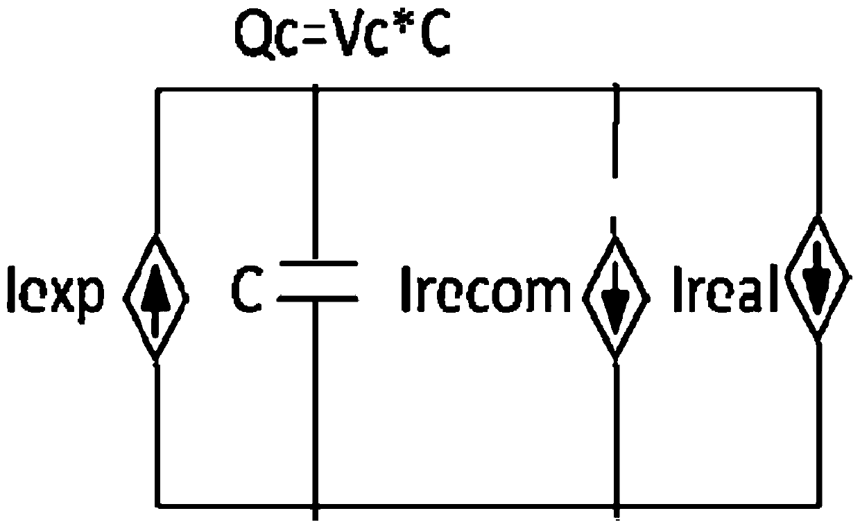
[0053] Step 1: Build a Subcircuit Model of the Single Event Effect Circuit

[0054] figure 1 Shown is a schematic diagram of a subcircuit model that includes an input componen...


PUM


Abstract

The invention relates to a modeling method considering node voltage dynamic change in single event effect circuit simulation. According to the method, the node voltage dynamic change condition in single event effect circuit simulation is described on the basis of a semi-physical-semi-analytical modeling thought, so that the single event effect sensitivity of the circuit is more reasonably and accurately predicted. The method mainly comprises the following steps: 1) constructing a sub-circuit model of the single event effect circuit; 2) acquiring current sources Iexp of different LET values anddifferent incident positions under the condition of connecting a constant bias voltage for the single tube; 3) calibrating by using a single-drive capability inverter to obtain a corresponding intermediate term fitting parameter frecomb and an output current source fitting parameter freal when heavy ions enter the N-type single-tube model and the P-type single-tube model; and 4) injecting the instantaneous current source modulated by the sub-circuit model into a working node in an actual circuit, and executing circuit simulation.

Description

technical field [0001] The invention relates to a single event effect simulation evaluation and reinforcement verification technology of a CMOS integrated circuit, in particular to a modeling method considering node voltage dynamic changes in single event effect circuit simulation. Background technique [0002] The single event effect of aerospace devices seriously affects the long-life and reliable operation of spacecraft in orbit. According to authoritative statistics, 45% of spacecraft on-orbit failures are caused by radiation damage, and single event effects account for more than 80% of radiation damage. Single event soft errors (single event upsets, single event transients) have become one of the important factors leading to on-orbit failures of spacecraft. [0003] Compared with the radiation test, the method of simulation analysis can predict the radiation resistance performance of the integrated circuit at the early stage of design, and then provide the basis for mo...

Claims


Application Information

Patent Timeline
Patent Type & Authority Applications(China)
IPC IPC(8): G06F30/367
CPCY02E60/00
Inventor 丁李利陈伟王坦张凤祁罗尹虹郭晓强王勋潘霄宇王定洪赵雯
Owner NORTHWEST INST OF NUCLEAR TECH
Why Eureka
Try Eureka