

Lossless screening method and device of radiation resisting capacity of GaN light-emitting diode
A light-emitting diode and screening method technology, applied in the field of microelectronics, can solve the problems of destructive detection, prolonging the development and production cycle, and inaccurate regression prediction equations, etc., and achieve the effect of efficient screening
- Summary
- Abstract
- Description
- Claims
- Application Information
AI Technical Summary
Problems solved by technology
Method used
Image

Examples
Embodiment Construction
[0037] The following will clearly and completely describe the technical solutions in the embodiments of the present invention with reference to the accompanying drawings in the embodiments of the present invention. Obviously, the described embodiments are only some, not all, embodiments of the present invention. The components of the embodiments of the invention generally described and illustrated in the figures herein may be arranged and designed in a variety of different configurations. Accordingly, the following detailed description of the embodiments of the invention provided in the accompanying drawings is not intended to limit the scope of the claimed invention, but merely represents selected embodiments of the invention. Based on the embodiments of the present invention, all other embodiments obtained by those skilled in the art without making creative efforts belong to the protection scope of the present invention.
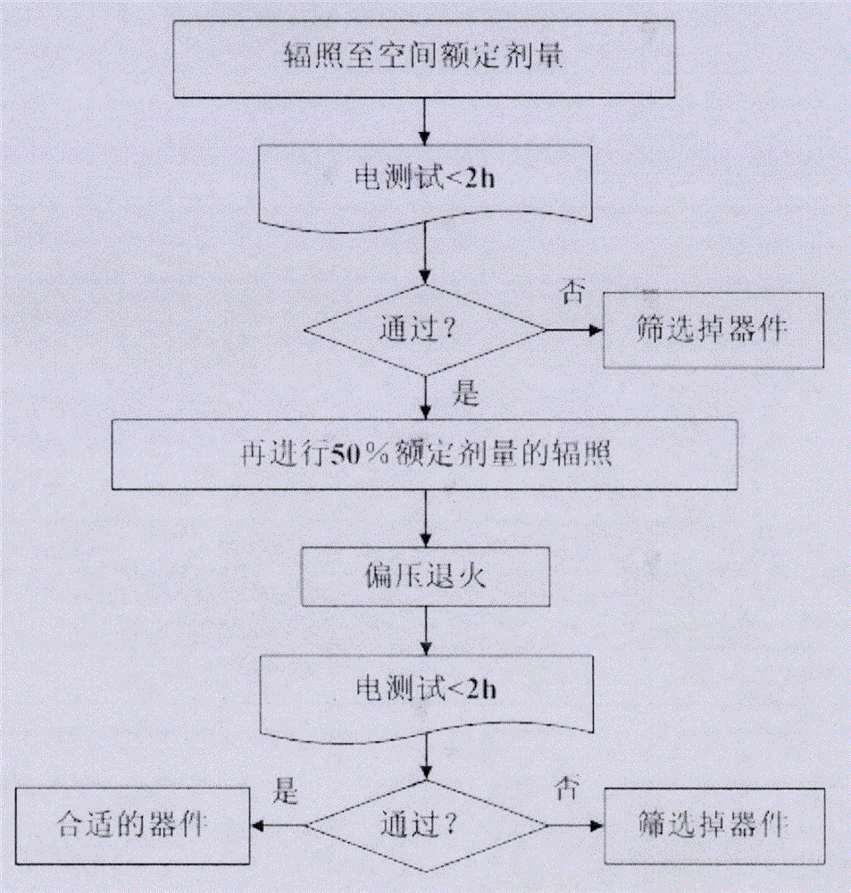
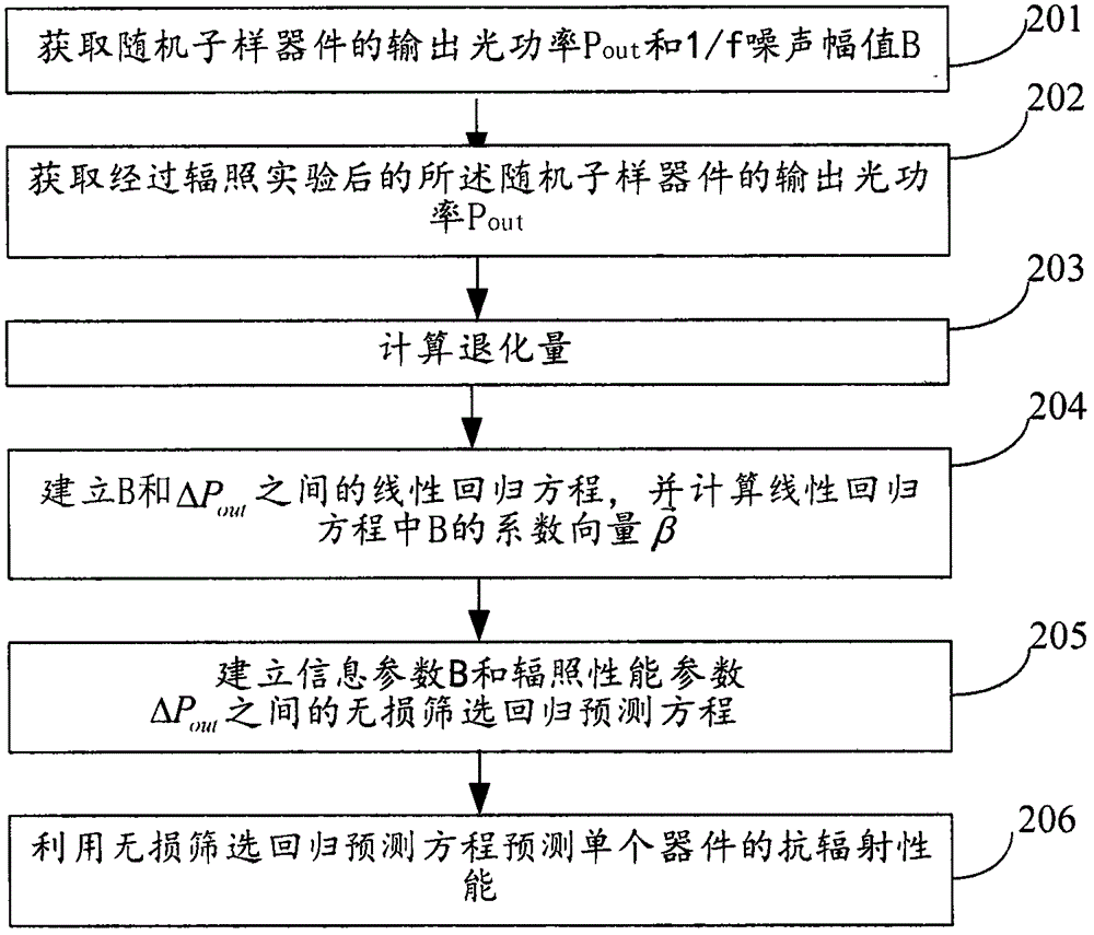
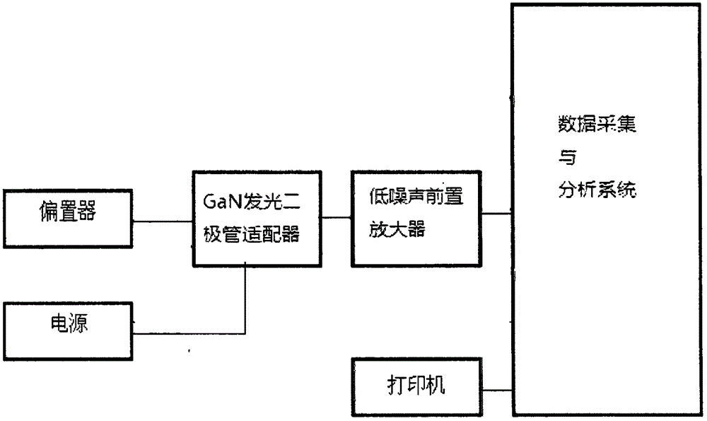
[0038]GaN light-emitting diodes need to be tested fo...
PUM
 Abstract
Description
Claims
Application Information