

Miniature light-emitting diode display panel and manufacturing method thereof
A technology of light-emitting diodes and display panels, applied to static indicators, instruments, electrical components, etc., can solve the problems of metal wire printing and alignment in mobile printing, and achieve high-precision effects
- Summary
- Abstract
- Description
- Claims
- Application Information
AI Technical Summary
Problems solved by technology
Method used
Image

Examples
Embodiment approach
[0071] In a specific implementation manner, the specific steps of forming openings corresponding to the signal lines one-to-one and metal film connection parts in the preset edge area may be as follows: Figure 7 , Figure 8a-8d Shown:
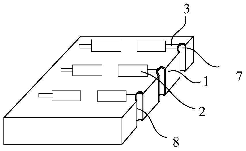
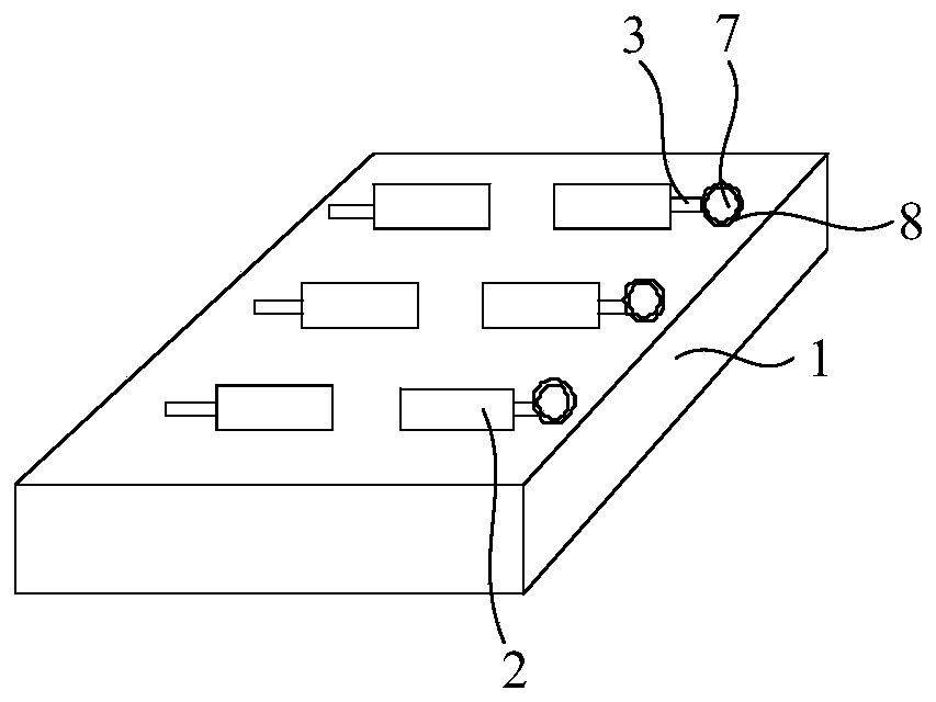
[0072] S701: Form a plurality of through holes corresponding to the signal lines in the preset edge area, and the centers of the plurality of through holes are on the same cutting line; specifically, as Figure 8a As shown, in the structure formed in this step, there are through holes 5 corresponding to the signal lines 3 in the predetermined edge region of the base substrate 1;
[0073] S702: Plating a metal film on at least the sidewall of the through hole; if Figure 8b As shown, there is a metal film 6 on the side wall of the through hole 5;
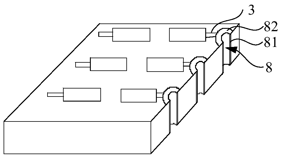
[0074] S703: Cut the base substrate along the cutting line to form the opening in the shape of a half hole and the connection part of the metal film; as Figure 8c As shown, the substrate is cut ...
PUM
| Property | Measurement | Unit |
|---|---|---|
| Diameter | aaaaa | aaaaa |
| Thickness | aaaaa | aaaaa |
Abstract
Description
Claims
Application Information