Mini LED chip and manufacturing method thereof

A manufacturing method and chip technology, which can be applied to electrical components, circuits, semiconductor devices, etc., can solve the problem of display device thickness, achieve the effects of large area, avoid poor flatness, and improve luminous efficiency

Inactive Publication Date: 2020-03-27
XIAMEN CHANGELIGHT CO LTD
View PDF0 Cites 8 Cited by
  • Summary
  • Abstract
  • Description
  • Claims
  • Application Information

AI Technical Summary

Problems solved by technology

However, since the LCD itself does not emit light, it needs to be coupled with an external light source to achieve display, resulting in a relatively thick display device for the LCD

Method used


Image

  • Mini LED chip and manufacturing method thereof
  • Mini LED chip and manufacturing method thereof
  • Mini LED chip and manufacturing method thereof

Examples


Embodiment Construction

[0038] The following will clearly and completely describe the technical solutions in the embodiments of the present invention with reference to the accompanying drawings in the embodiments of the present invention. Obviously, the described embodiments are only some, not all, embodiments of the present invention. Based on the embodiments of the present invention, all other embodiments obtained by persons of ordinary skill in the art without making creative efforts belong to the protection scope of the present invention.

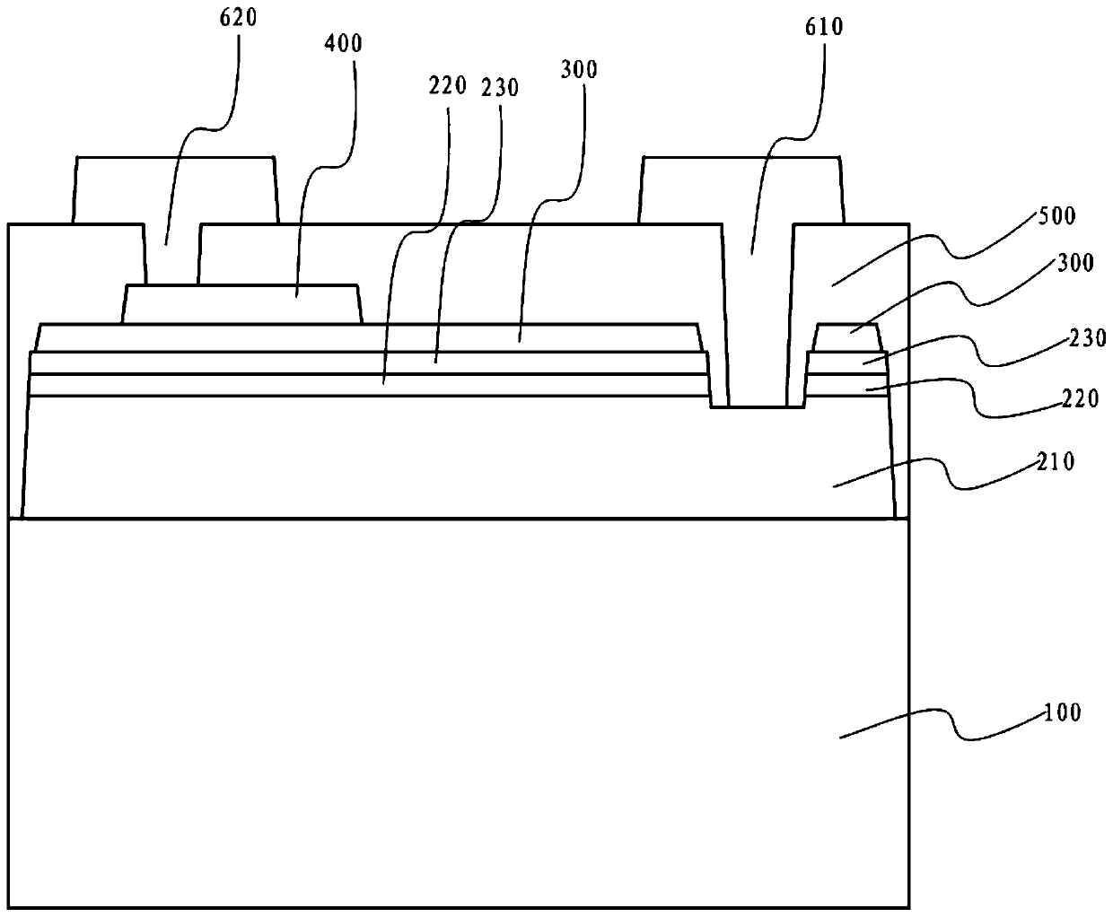
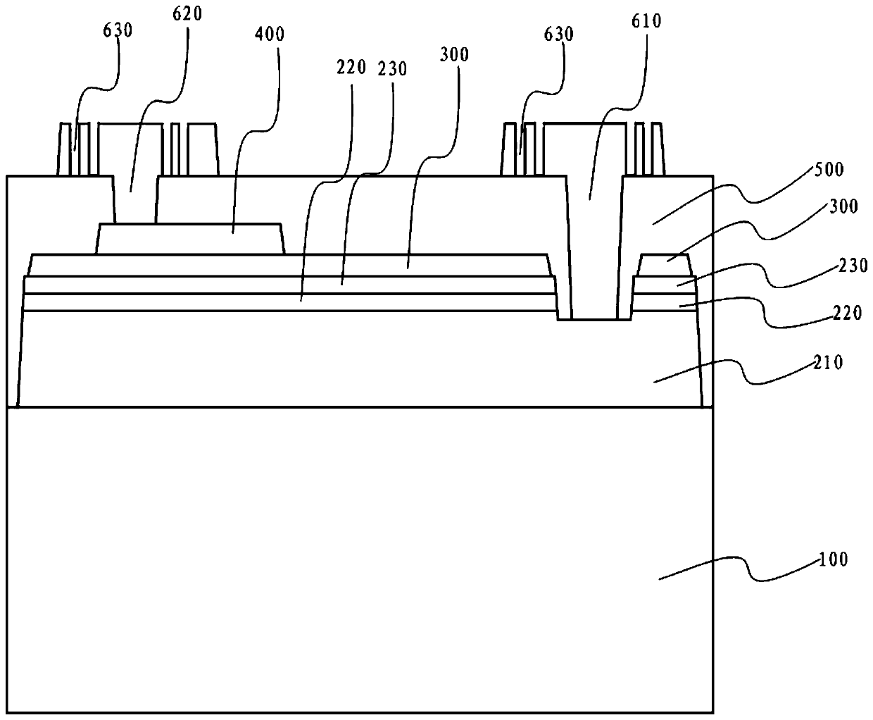
[0039]As mentioned in the background technology, with the upgrading of display panels, a new type of display panel-micro-light-emitting diode (Mini LED) display panel has appeared on the market, which is also an active light-emitting device, and compared with OLED display panels , with faster response speed, wider operating temperature range, higher light source utilization, longer life, and lower cost, these advantages make micro-LED display panels expected to...


PUM

PropertyMeasurementUnit
thicknessaaaaaaaaaa

Abstract

The invention provides a Mini LED chip and a manufacturing method thereof. The first auxiliary extension electrodes are located between the first type semiconductor layer and the first bonding electrodes and are not connected through the corresponding auxiliary extension electrodes. That is to say, no auxiliary extension electrode is manufactured on the surface of the exposed first-type semiconductor layer at the electrode contact hollowed-out part, so that the problem that the area occupied by the electrode contact hollowed-out part is enlarged due to the existence of the auxiliary extensionelectrode is avoided, the area of a light-emitting region is large, and the light-emitting efficiency of the Mini LED chip is improved. Further, according to the technical scheme provided by the invention, an auxiliary extension electrode does not need to be manufactured; therefore, the problems that the flatness of the prepared first bonding electrode is poor and the coverage effect of the insulation isolation reflection layer is poor due to the existence of the auxiliary expansion electrode are avoided, the reliability of the Mini LED chip is improved, and the light-emitting angle of the Mini LED chip is ensured to achieve an expected effect at the same time.

Description

technical field [0001] The present invention relates to the technical field of semiconductor devices, and more specifically, to a Mini LED (Mini LightEmitting Diode, Micro Light Emitting Diode) chip and a manufacturing method thereof. Background technique [0002] Liquid Crystal Display (LCD) has the advantages of light weight, thin thickness, easy driving, and no harmful rays, and is widely used in modern information equipment such as TVs, notebook computers, and mobile phones. However, since the LCD itself does not emit light, it needs to be coupled with an external light source to achieve display, resulting in a relatively thick display device for the LCD. In order to adapt to the development trend of thinner and lighter display panels, organic light-emitting diode (Organic Light-Emitting Diode, OLED) display panels appeared after LCD, which have self-illumination, no backlight, high contrast, thin thickness, and fast response. , Can be used for excellent characteristics...

Claims


Application Information

Patent Timeline
Patent Type & Authority Applications(China)
IPC IPC(8): H01L33/46H01L33/38H01L33/00
CPCH01L33/005H01L33/382H01L33/46
Inventor 刘英策李俊贤刘兆黄瑄邬新根
Owner XIAMEN CHANGELIGHT CO LTD
Why Eureka
Try Eureka