Eureka AIR delivers breakthrough ideas for toughest innovation challenges, trusted by R&D personnel around the world.

Feed network device and antenna

A feed network and feed network technology, applied in the field of feed network devices and antennas, can solve the problems of large dielectric constant deviation, inability to feed network devices, and high cost

Active Publication Date: 2020-03-31
COMBA TELECOM TECH (GUANGZHOU) CO LTD
View PDF11 Cites 0 Cited by
  • Summary
  • Abstract
  • Description
  • Claims
  • Application Information

AI Technical Summary

Problems solved by technology

Among them, PTFE has a low dielectric constant and low dielectric loss, making it the preferred high-frequency PCB material, but the cost is high; in addition, the dielectric loss tangent of the lower-cost epoxy resin board is 10 times that of ordinary materials, and the dielectric loss The electric constant deviation is large, so it cannot be used to make a feed network device

Method used


Image

  • Feed network device and antenna
  • Feed network device and antenna
  • Feed network device and antenna

Examples


Embodiment Construction

[0034] In order to make the above objects, features and advantages of the present invention more comprehensible, specific implementations of the present invention will be described in detail below in conjunction with the accompanying drawings. In the following description, numerous specific details are set forth in order to provide a thorough understanding of the present invention. However, the present invention can be implemented in many other ways different from those described here, and those skilled in the art can make similar improvements without departing from the connotation of the present invention, so the present invention is not limited by the specific embodiments disclosed below.

[0035] In the description of the present invention, it should be understood that the terms "first" and "second" are used for description purposes only, and cannot be interpreted as indicating or implying relative importance or implicitly indicating the quantity of indicated technical featu...


PUM


Abstract

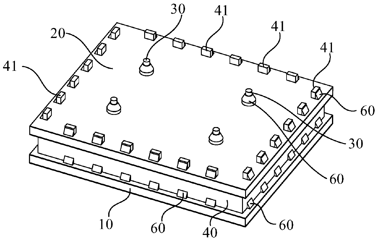
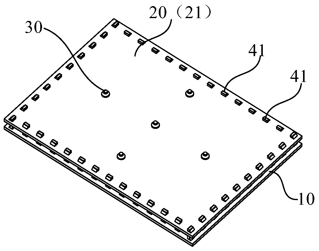
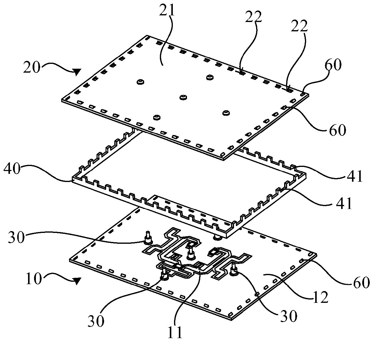
The invention relates to a feed network device and an antenna. The feed network device comprises a feed network plate, a cover plate and a support column. Aa feed network line is arranged on the surface of one side of the feed network plate. The cover plate is connected with the feed network plate through the support columns, and a first grounding metal layer is arranged on the side surface, facing the feed network plate, of the cover plate. The feed network line faces the first grounding metal layer, and a gap is arranged between the feed network line and the first grounding metal layer. Airbetween the feed network plate and the cover plate is used as a medium, and an air microstrip mode is adopted, so that the cost can be reduced. The supporting columns can control the distance betweena feed network line and the ground, it is guaranteed that a traditional feed network device can be simulated, and the good performance of the traditional feed network device is reserved. Compared witha traditional feed network device of a four-layer plate structure, the thickness of the feed network device can be reduced due to the fact that the number of layers is reduced, and therefore the lowprofile can be achieved, and the physical space size can be reduced under the condition that it is guaranteed that indexes are qualified.

Description

technical field [0001] The invention relates to the technical field of communication, in particular to a feeding network device and an antenna. Background technique [0002] In the coverage of mobile communication networks, the 5G Massive MIMO antenna is one of the key devices of the coverage network, and the gain of the antenna depends on the loss of the feeding network. Since the dielectric loss tangent of the dielectric material determines the loss of the power divider of the feed network device, PCB boards with low dielectric loss are the research focus of major board manufacturers. [0003] A general feeding network device uses a high-frequency PCB (specifically made of PTFE) as a power divider and is placed on the bottom plate. The high-frequency PCB usually includes an upper layer, an intermediate line layer, and a lower layer arranged in sequence. The PP dielectric layer is bonded to the base plate, and the high-frequency PCB board and the base plate are connected t...

Claims


Application Information

Patent Timeline
IPC IPC(8): H01Q1/50H01Q1/48H01Q1/52
CPCH01Q1/48H01Q1/50H01Q1/526
Inventor 陈礼涛高彬黄明达李轶帆
Owner COMBA TELECOM TECH (GUANGZHOU) CO LTD
Why Eureka
Eureka Blog
Learn More