Semiconductor device test fixture and test box body

A technology for testing fixtures and semiconductors, which is used in the testing of single semiconductor devices, parts and instruments of electrical measuring instruments, etc., can solve the problems of manual tightening of screws, time-consuming and labor-intensive, etc., to achieve convenient and detachable connections, improve work efficiency, and facilitate detection. effect used

Pending Publication Date: 2020-04-03
HEFEI KEWELL POWER SYST CO LTD
View PDF0 Cites 2 Cited by
  • Summary
  • Abstract
  • Description
  • Claims
  • Application Information

AI Technical Summary

Problems solved by technology

[0004] The technical problem to be solved by the present invention is to provide a semiconductor device test fixture and a test box to solve the time-consuming and labor-intensive problem of manually tightening the screws when the test fixture is connected to the device under test;

Method used


Image

  • Semiconductor device test fixture and test box body
  • Semiconductor device test fixture and test box body
  • Semiconductor device test fixture and test box body

Examples


Embodiment 2

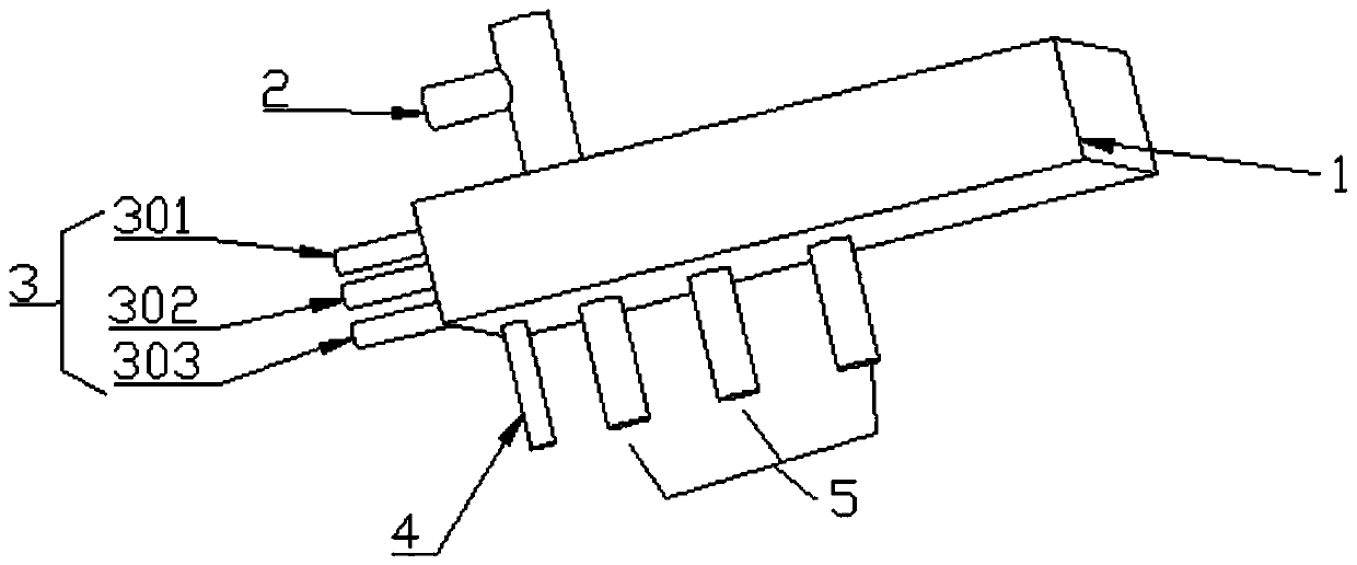
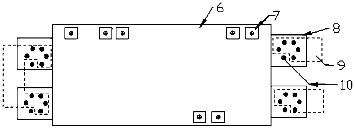
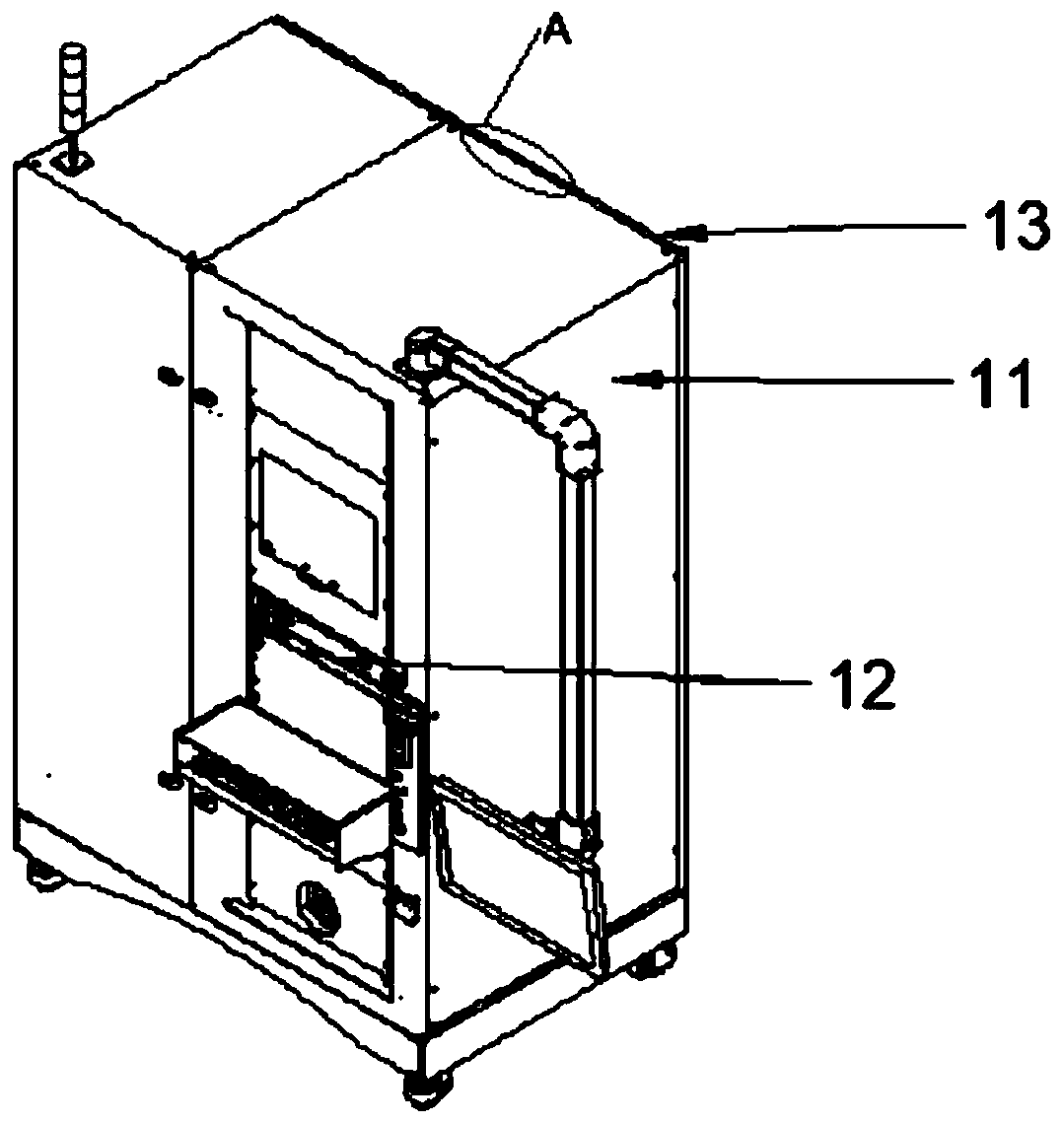
[0037] Such as Figure 3-Figure 4 , image 3 Schematic diagram of the axial side of the semiconductor device test box; Figure 4 for image 3 An enlarged schematic diagram of the rear view of middle A; a semiconductor device test box, including a box body 11, a semiconductor device test automation tool 12, a laminated busbar connection device 13, and a semiconductor device test fixture,

[0038] The box body 11 is provided with a stretchable semiconductor device test automation tool 12 inside the lower right side of the front side, and the rear side wall of the box body 11 is provided with a laminated busbar connection device 13, and the laminated mother The row connecting device 13 is connected to the semiconductor device test fixture through a probe, the semiconductor device test fixture is connected to the DUT 6 through a probe, the semiconductor device test fixture is set on the top of the semiconductor device test automation tool 12, and The semiconductor device test fixture...


PUM


Abstract

A semiconductor device test fixture disclosed by the present invention comprises an epoxy plate, a first signal probe, a first connecting end, a second signal probe and a second connecting end, wherein the first connecting end is arranged on one side of the epoxy plate, the position, close to the first connecting end, of the top of the epoxy plate is connected with the first signal probe through aconnecting column body, and the second signal probe is further arranged at the bottom of the epoxy plate, and a second connecting end is arranged at the position, at one side of the second signal probe, of the bottom of the epoxy plate. The invention also discloses a semiconductor test box body. When the test fixture is used, the first signal probe of the test fixture is connected with a third connecting point, the second connecting end is connected with a second connecting point, and the second signal probe is connected with the first connecting point of a tested piece, so that the tested piece is connected with the test fixture. When the test fixture is used, the test fixture is convenient to detect and use, is time-saving and labor-saving, and is convenient to disassemble.

Description

Technical field [0001] The invention relates to the technical field of power electronic device testing, and more specifically to a semiconductor device testing fixture and a testing box. Background technique [0002] The rapid development of industry has resulted in corresponding developments in many industries. The semiconductor industry is one of the most important. People have continuously deepened research on semiconductor products, and their performance has been further improved. In the process of researching and analyzing semiconductors, in order to ensure that the role of semiconductors in the application process can be fully utilized, higher requirements are put forward for its testing. In the process of testing semiconductors, it is necessary to adopt a reasonable clamping method and a reasonable movement method before and after the test of the device, so as to achieve an efficient mode. [0003] In the study of the characteristics of semiconductors (such as IGBTs), the s...

Claims


Application Information

Patent Timeline
Patent Type & Authority Applications(China)
IPC IPC(8): G01R31/26G01R1/04
CPCG01R1/0425G01R31/2601
Inventor 韩正柏加来朱国军唐德平
Owner HEFEI KEWELL POWER SYST CO LTD
Why Eureka
Try Eureka