Semiconductor structure and forming method thereof

A technology of semiconductor and gate structure, applied in the field of semiconductor structure and its formation, can solve the problem of easy breakdown of FinFET, and achieve the effect of improving the ability to resist breakdown

Active Publication Date: 2020-04-03
SEMICON MFG INT (SHANGHAI) CORP +1
View PDF20 Cites 4 Cited by
  • Summary
  • Abstract
  • Description
  • Claims
  • Application Information

AI Technical Summary

Problems solved by technology

[0004] The source-drain doped layers on both sides of the FinFET gate structure are formed by epitaxy, which can enhance the device performance of the FinFET, but the FinFET has the problem of being easily broken down.

Method used


Image

  • Semiconductor structure and forming method thereof
  • Semiconductor structure and forming method thereof
  • Semiconductor structure and forming method thereof

Examples


Embodiment Construction

[0032] It can be seen from the background technology that when the source-drain doped layer is formed by epitaxial method, the FinFET is easy to be broken down. Now, combining with a method of forming a semiconductor structure, it is analyzed that the source-drain doped layer is formed by epitaxial method. The reason why the top is easy to be broken down.

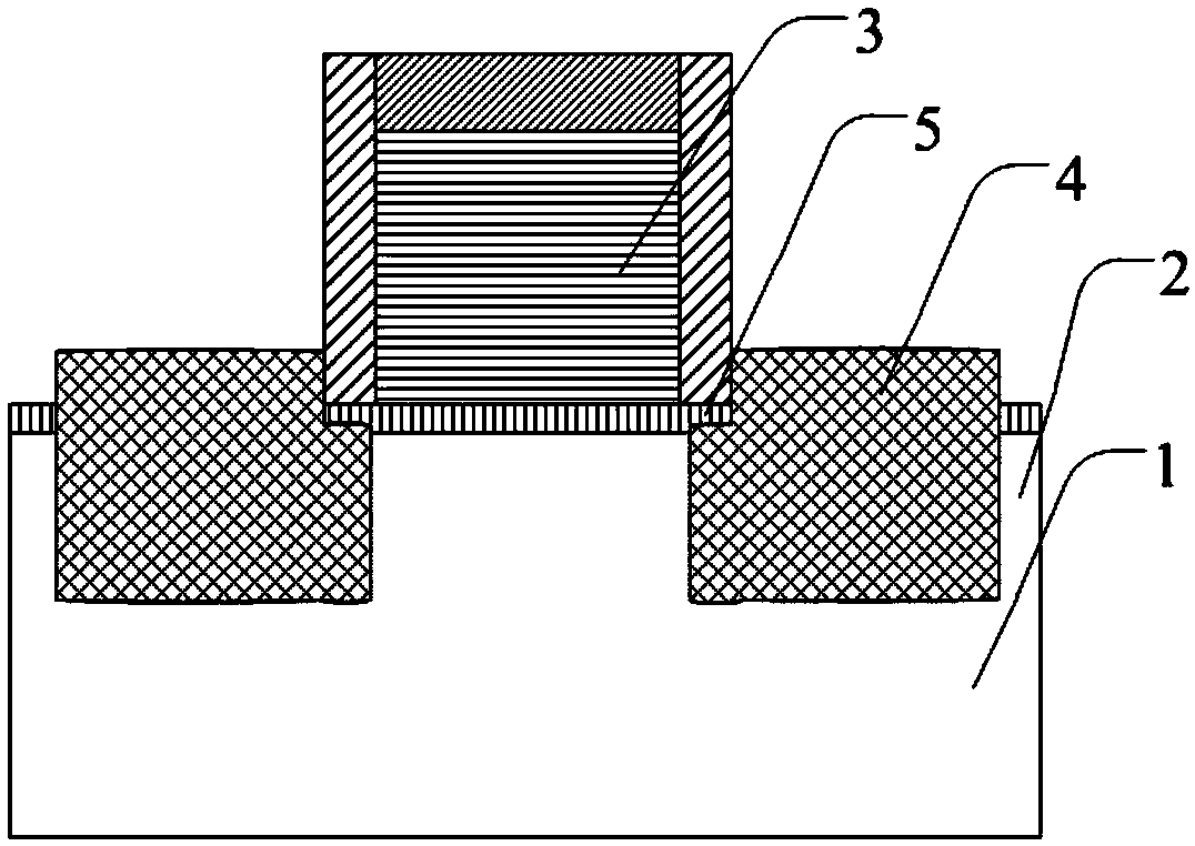
[0033] refer to figure 1 , shows a structural schematic diagram corresponding to a method for forming a semiconductor structure.

[0034] Such as figure 1 As shown, a base is provided, and the base includes a substrate 1, a fin 2 separated on the substrate 1, a gate structure 3 across the fin 2, and fins located on both sides of the gate structure 3. The source-drain doped layer 4 in part 2, the gate structure 3 covers part of the top surface and part of the sidewall of the fin part 2, and an oxide layer is formed between the gate structure 3 and the fin part 2 Layer 5.

[0035] In this embodiment, the channel is a U-sh...


PUM

PropertyMeasurementUnit
thicknessaaaaaaaaaa
depthaaaaaaaaaa
depthaaaaaaaaaa

Abstract

The invention provides a semiconductor structure and a forming method thereof. The forming method comprises the steps that a base is provided, the base comprises a substrate, fin parts separately arranged on the substrate and a gate structure stretching across the fin parts, and the gate structure covers part of the top surfaces and part of the side walls of the fin parts; partial thickness of thefin parts on two sides of the gate structure are removed, grooves located in the two sides of the gate structure are formed, each groove comprises a first groove and a second groove located in the bottom end of the first groove, each first groove comprises a first side wall close to the gate structure, each second groove comprises a second side wall close to the gate structure, and each second side wall is located on the side, close to the gate structure, of the corresponding first side wall; and source-drain doped layer is formed in the grooves. According to the embodiment of the invention,the fin parts below the gate structure are used as channels, because the second grooves are located at the bottom ends of the first grooves, the distance between the source-drain doped layer located in the second grooves and the gate structure is relatively long, and it is not easy to diffuse doped ions in the source-drain doped layer to the gate structure, so that the breakdown resistance of thesemiconductor structure is improved.

Description

technical field [0001] The invention relates to the technical field of semiconductors, in particular to a semiconductor structure and a forming method thereof. Background technique [0002] In semiconductor manufacturing, with the development trend of ultra-large-scale integrated circuits, the feature size of integrated circuits continues to decrease. In order to adapt to smaller feature sizes, metal-oxide-semiconductor field-effect transistors (Metal-Oxide-Semiconductor Field-Effect Transistor , MOSFET) channel length has been shortened accordingly. However, as the channel length of the device is shortened, the distance between the source and the drain of the device is also shortened, so the ability of the gate structure to control the channel becomes worse, and the gate voltage pinches off the channel. The channel becomes more and more difficult, making subthreshold leakage (subthreshold leakage), the so-called short-channel effect (SCE: short-channel effects) more likely...

Claims


Application Information

Patent Timeline
Patent Type & Authority Applications(China)
IPC IPC(8): H01L21/336H01L29/08H01L29/78
CPCH01L29/66795H01L29/785H01L29/0847
Inventor 周飞
Owner SEMICON MFG INT (SHANGHAI) CORP
Why Eureka
Try Eureka