Method for taking physical property fault analysis test piece of semiconductor device

A fault analysis, semiconductor technology, applied in sampling devices and other directions, can solve the problems of poor accuracy, low efficiency, and a lot of time, so as to reduce the time of thinning, improve flexibility, and alleviate by-products.

Pending Publication Date: 2020-04-07
CHANGXIN MEMORY TECH INC
View PDF9 Cites 0 Cited by
  • Summary
  • Abstract
  • Description
  • Claims
  • Application Information

AI Technical Summary

Problems solved by technology

However, this method is very simple and has poor precision. The sample cut by wire saw can only be called a rough sample. It takes a lot of time to do the thinning process in the TEM detection process, which is obviously inefficient.

Method used


Image

  • Method for taking physical property fault analysis test piece of semiconductor device
  • Method for taking physical property fault analysis test piece of semiconductor device
  • Method for taking physical property fault analysis test piece of semiconductor device

Examples


Embodiment Construction

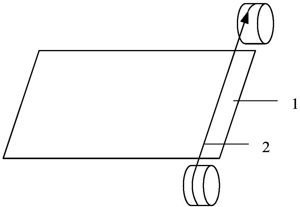
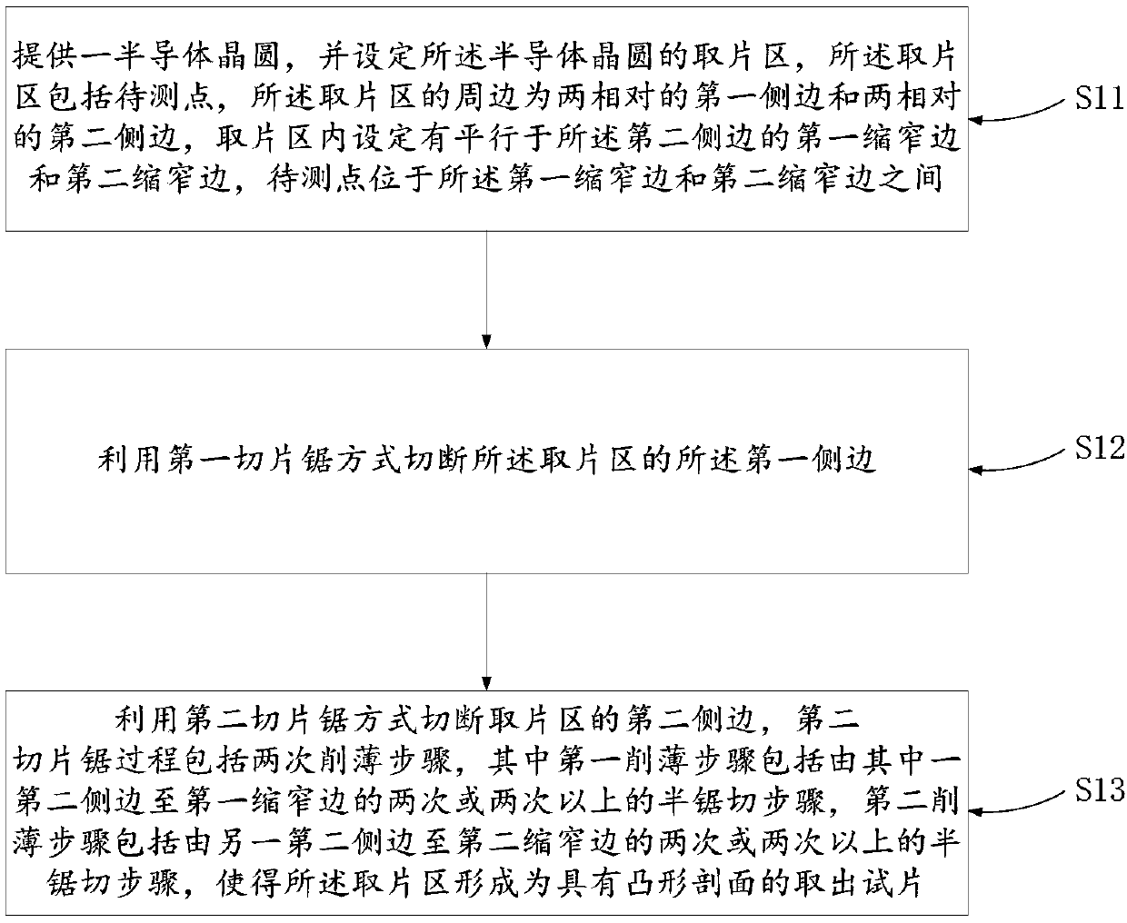
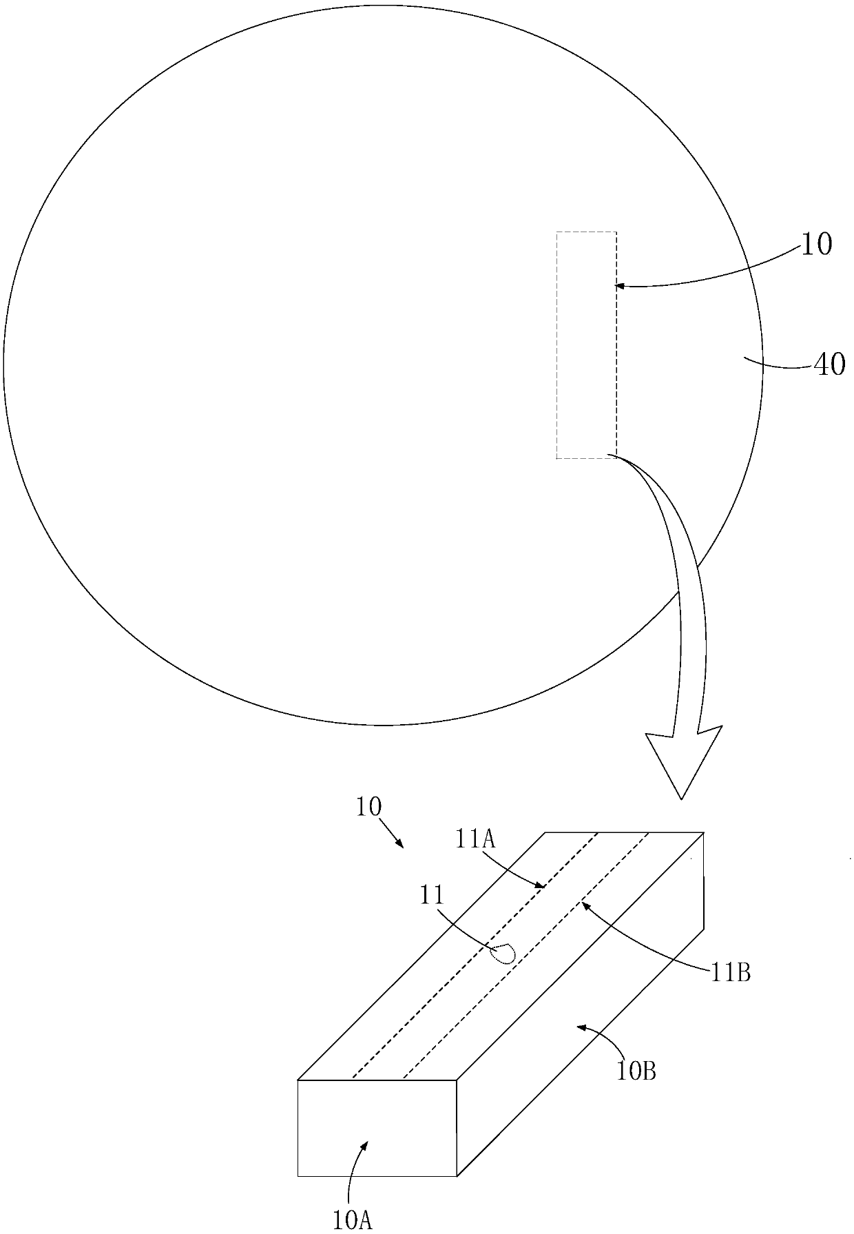
[0040] Below will be described in more detail the taking method of the semiconductor device physical failure analysis test piece of the present invention in conjunction with schematic diagram, wherein represents preferred embodiment of the present invention, should understand that those skilled in the art can modify the present invention described here, and The advantageous effects of the invention are still achieved. Therefore, the following description should be understood as the broad knowledge of those skilled in the art, but not as a limitation of the present invention.

[0041] In the following paragraphs the invention is described more specifically by way of example with reference to the accompanying drawings. Advantages and features of the present invention will be apparent from the following description and claims. It should be noted that all the drawings are in a very simplified form and use imprecise scales, and are only used to facilitate and clearly assist the pu...


PUM

PropertyMeasurementUnit
widthaaaaaaaaaa
heightaaaaaaaaaa

Abstract

The invention provides a method for taking a physical property fault analysis test piece of a semiconductor device. According to the method for taking the physical property fault analysis test piece of the semiconductor device, a half sawing step is sequentially executed from one side edge to a first narrowing edge of a piece taking area and from a second narrowing edge to the other side edge of the piece taking area, so that the taking-out test piece with a convex section is formed. Therefore, the obtained boundary of the taken-out test piece can reach the target position more easily, the FIBthinning time can be shortened, byproducts generated during FIB thinning can be relieved, a sample can be reworked, and thus the flexibility of sample preparation is improved.

Description

technical field [0001] The invention relates to the field of sample detection, in particular to a method for taking a semiconductor device physical property failure analysis test piece. Background technique [0002] In semiconductor integrated circuits, Physical Failure Analysis (PFA) usually uses TEM (Transmission Electron Microscope) to obtain TEM photos of the structure to be tested in the chip, and obtain characteristics such as the shape or size of the structure to be tested based on the TEM photos. At the same time, TEM has the advantages of high magnification and high resolution, making it widely used in the fields of process control or failure analysis. [0003] When using TEM to analyze the characteristics of the structure to be tested, the preparation of TEM samples is a very important part. In order to obtain TEM pictures with sufficient brightness and contrast, the TEM sample must be thin enough (generally less than 100nm) so that electrons can pass through the ...

Claims


Application Information

Patent Timeline
Patent Type & Authority Applications(China)
IPC IPC(8): G01N1/04
CPCG01N1/04
Inventor 不公告发明人
Owner CHANGXIN MEMORY TECH INC
Why Eureka
Try Eureka