Chip surface defect classification device and method based on generative adversarial network

A defect classification and generative technology, applied in biological neural network models, measurement devices, neural learning methods, etc., can solve the problem of difficult to meet the training data demand of deep convolutional neural network, can not effectively improve the classification performance of recognition models, defect pictures Issues such as limited quantity, to achieve the effect of improving classification accuracy, improving classification efficiency, and improving training accuracy

Inactive Publication Date: 2020-04-10
SHANGHAI INTEGRATED CIRCUIT RES & DEV CENT
View PDF5 Cites 9 Cited by
  • Summary
  • Abstract
  • Description
  • Claims
  • Application Information

AI Technical Summary

Problems solved by technology

However, in actual production, due to the limited number of defect images generated online, it is difficult to meet the large demand for deep convolutional neural network training data; if the number of defect images used for training is insufficient, the accuracy of the model will be affected
Traditional image enhancement methods based on captured image processing and changes only generate new images based on limited invariance, and the generalization ability is weak, which cannot effectively improve the classification performance of the recognition model

Method used


Image

  • Chip surface defect classification device and method based on generative adversarial network
  • Chip surface defect classification device and method based on generative adversarial network
  • Chip surface defect classification device and method based on generative adversarial network

Examples


Embodiment 1

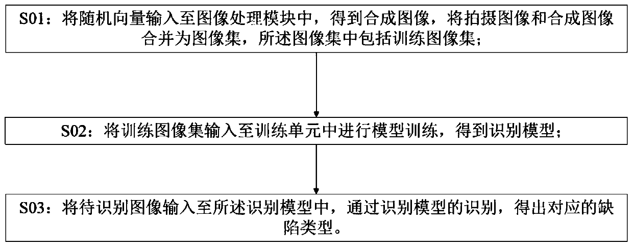
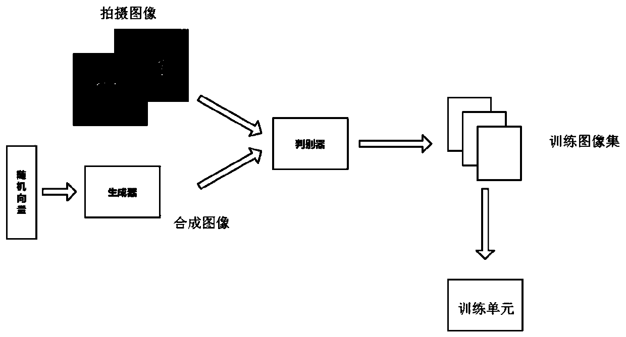
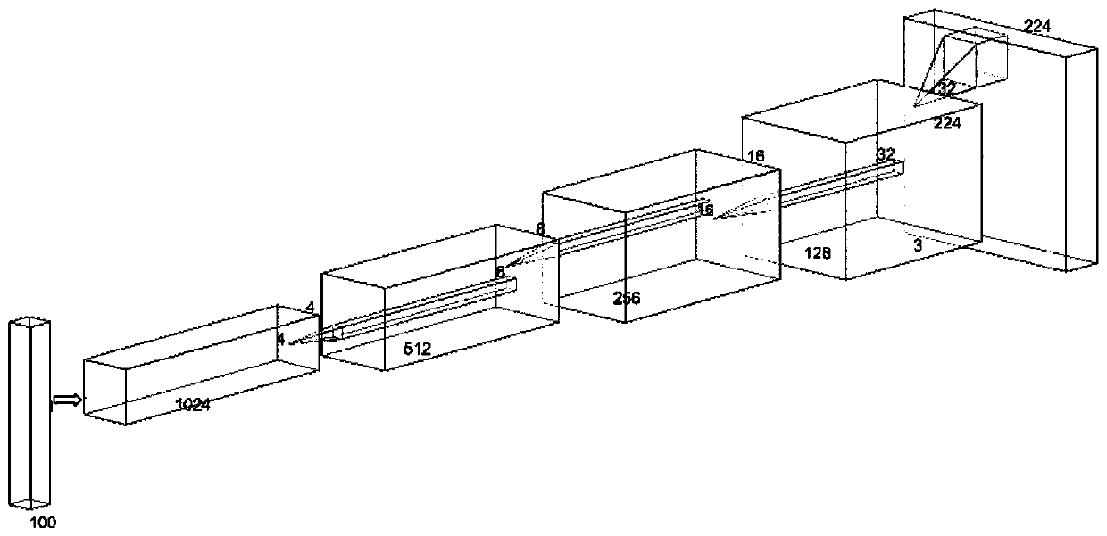
[0054] The image processing module in the present invention includes a generative confrontation network. When both the generator and the judger are units based on the convolutional neural network, the input and output schematic diagram of the generator is shown in the attached image 3 As shown, the input and output schematic diagram of the judge is as attached Figure 4 As shown, the specific steps for the generator and the judger to generate a composite image in the image processing module are as follows:

[0055] T01: Input the random vector into the input layer of the generator, the size of the input layer of the generator is 100×1; in this embodiment, the size of the input layer of the generator is set according to the defect type of the synthesized image, and can also be other values;

[0056] T02: The synthetic image output by the input layer of the generator is input to the first convolutional layer GC1 of the generator. The size of the first convolutional layer GC1 of...


PUM


Abstract

The invention discloses a chip surface defect classification method based on a generative adversarial network. The method comprises the following steps: S01, inputting a random vector into an image processing module, obtaining a composite image, combining a photographed image and the composite image into an image set, and enabling the image set to comprise a training image set; s02, inputting thetraining image set into a training unit for model training to obtain a recognition model; and S03, inputting a to-be-recognized image into the recognition model, and obtaining a corresponding defect type through recognition of the recognition model. According to the chip surface defect classification device and method based on the generative adversarial network provided by the invention, the synthetic image is generated by using the random vector, and the synthetic image is used as one part of the image set, so that a large number of training images and test images are formed, and the trainingaccuracy and generalization ability of a recognition model are improved.

Description

technical field [0001] The invention relates to the field of machine vision, in particular to a chip surface defect classification device and method based on a generative confrontation network. Background technique [0002] Integrated circuit chips are widely used in various fields and are the key to national economic development and information security. However, during the manufacturing process of its package, the defects generated on the chip surface will directly affect the working life and reliability. Traditional manual detection and classification methods have shortcomings such as relying on subjective experience, time-consuming and labor-consuming, and high false detection rate, which can no longer meet the needs of high-precision and high-speed production lines. [0003] The traditional chip defect classification technology based on machine vision has a relatively mature framework system, which includes the following processes in turn: image acquisition, defect ima...

Claims


Application Information

Patent Timeline
Patent Type & Authority Applications(China)
IPC IPC(8): G06T7/00G06K9/62G06N3/04G06N3/08G01N21/88G01N21/956
CPCG06T7/0004G06N3/08G01N21/8851G01N21/956G06T2207/10004G06T2207/20081G06T2207/20084G06T2207/30148G01N2021/8854G01N2021/95638G06N3/045G06F18/241
Inventor 傅豪王鹏飞李琛段杰斌周涛王修翠余学儒
Owner SHANGHAI INTEGRATED CIRCUIT RES & DEV CENT
Why Eureka
Try Eureka