Voltage control method and device during erasing of 3D NAND memory

A voltage control method and voltage control technology, applied in static memory, read-only memory, information storage, etc., can solve problems such as memory cell string current reduction, pseudo memory cell threshold voltage drift, and real memory cell read errors.

Active Publication Date: 2020-04-10
YANGTZE MEMORY TECH CO LTD
View PDF3 Cites 6 Cited by
  • Summary
  • Abstract
  • Description
  • Claims
  • Application Information

AI Technical Summary

Problems solved by technology

In the erasing operation, the voltage of the word line where the dummy memory cell is located is coupled to a high voltage by the well doped region, resulting in a shift in the threshold voltage of the dummy memory cell

Method used


Image

  • Voltage control method and device during erasing of 3D NAND memory
  • Voltage control method and device during erasing of 3D NAND memory
  • Voltage control method and device during erasing of 3D NAND memory

Examples


Embodiment Construction

[0045] In order to make the above objects, features and advantages of the present invention more clearly understood, the specific embodiments of the present invention will be described in detail below with reference to the accompanying drawings.

[0046] Many specific details are set forth in the following description to facilitate a full understanding of the present invention, but the present invention can also be implemented in other ways different from those described herein, and those skilled in the art can do so without departing from the connotation of the present invention. Similar promotion, therefore, the present invention is not limited by the specific embodiments disclosed below.

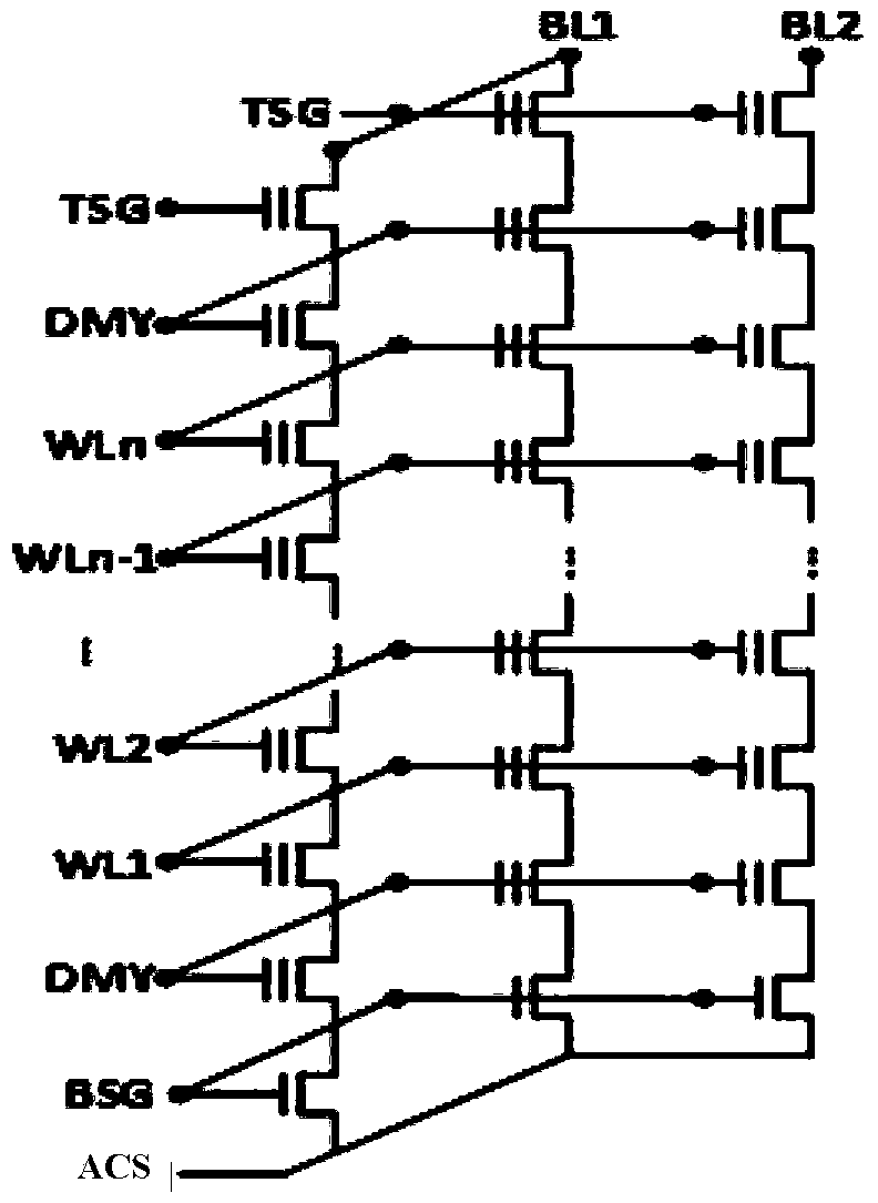
[0047] As described in the background art, in a 3D NAND memory, a memory array is formed by strings of memory cells, thereby forming memory cells in a three-dimensional direction. The memory cells used for storage are formed together and have basically the same structure. For the convenie...


PUM


Abstract

The invention provides a voltage control method during erasing of a 3D NAND memory. When the bias voltage of the word line of the true memory cell is at the erase control voltage; raising the bias voltage of the well doped region to an erase working voltage and keeping the erase working voltage; when the bias voltage of the well doped region rises to a first intermediate voltage, the well doped region is grounded; keeping the bias voltage of the word line of the pseudo memory cell at a first preset voltage, then, setting a word line of the pseudo memory unit to be in a floating state; whereinthe first preset voltage is smaller than the first intermediate voltage; thus, the voltage difference between the voltage of the word line where the pseudo memory cell is located and the voltage of the word line where the adjacent true memory cell is located is reduced; tunneling between the word line where the true memory unit is located and the word line where the pseudo memory unit is located is avoided, so that threshold voltage drift of the pseudo memory unit is avoided, reduction of string current of the memory unit is avoided, and reading errors of the true memory unit are avoided.

Description

technical field [0001] The present invention relates to the field of integrated circuit design of memory, in particular to a voltage control method and device during erasing of 3D NAND memory. Background technique [0002] NAND flash memory is a non-volatile storage product with low power consumption, light weight and good performance, and has been widely used in electronic products. In order to further increase the storage capacity and reduce the storage cost per bit, 3D NAND memory is proposed. [0003] In the 3D NAND memory, a memory array is formed by strings of memory cells to form memory cells in a three-dimensional direction, and the memory cell strings contain real memory cells that are actually used for storage and dummy memory cells that are not actually used for storage. When the erase operation of the memory cell is performed, the word line where the dummy memory cell is located is in a floating state. During the erasing operation, the voltage of the word line w...

Claims


Application Information

Patent Timeline
IPC IPC(8): G11C16/14G11C16/30G11C16/04
CPCG11C16/14G11C16/30G11C16/0483
Inventor 曹华敏付祥姜柯高帅陈子龙安阳向斌黄新运张黄鹏王颀
Owner YANGTZE MEMORY TECH CO LTD
Why Eureka
Try Eureka