Display substrate, display device and preparation method of display substrate

A display substrate and display device technology, which is applied in semiconductor/solid-state device manufacturing, semiconductor devices, electrical components, etc., can solve problems such as pad failure and pad short-circuit, and achieve the effect of increasing distance

Active Publication Date: 2020-04-10
KUNSHAN GO VISIONOX OPTO ELECTRONICS CO LTD
View PDF2 Cites 1 Cited by
  • Summary
  • Abstract
  • Description
  • Claims
  • Application Information

AI Technical Summary

Problems solved by technology

The inventors found that a short circuit is prone to occur between two pads arranged at intervals in the existing bonding area, resulting in failure of the pads

Method used


Image

  • Display substrate, display device and preparation method of display substrate
  • Display substrate, display device and preparation method of display substrate
  • Display substrate, display device and preparation method of display substrate

Examples


Embodiment Construction

[0027] In order to make the purpose, technical solutions and advantages of the embodiments of the present invention more clear, various implementation modes of the present invention will be described in detail below in conjunction with the accompanying drawings. However, those of ordinary skill in the art can understand that, in each implementation manner of the present invention, many technical details are provided for readers to better understand the present application. However, even without these technical details and various changes and modifications based on the following implementation modes, the technical solution claimed in this application can also be realized.

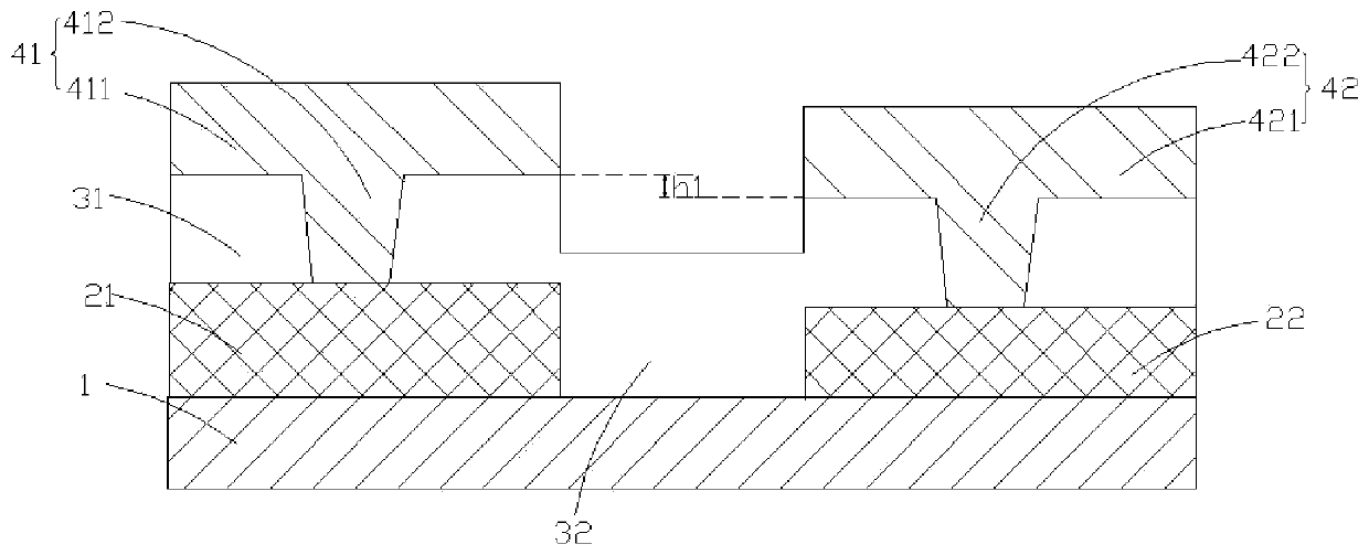
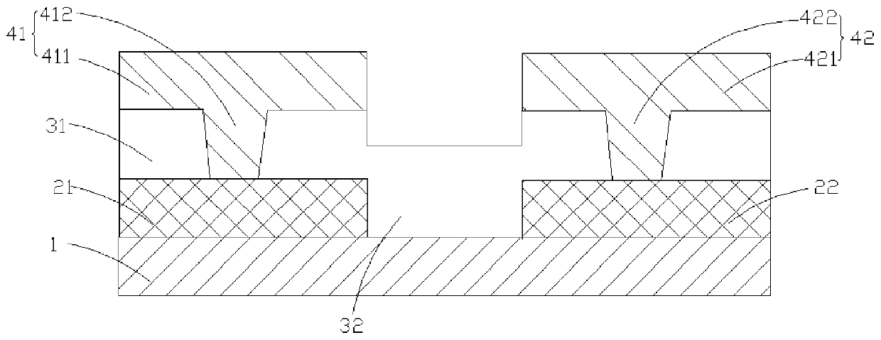
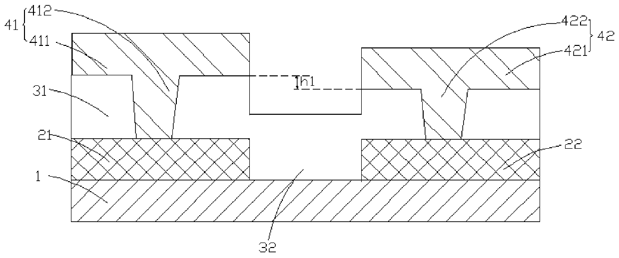
[0028] The first embodiment of the present invention relates to a display substrate, such as figure 1As shown, the core of this embodiment is the display substrate, including: a first metal layer 21 and a second metal layer 22 disposed on the substrate 1 at intervals; The first insulating layer 31 on one si...


PUM


Abstract

The embodiment of the invention relates to the technical field of display, and discloses a display substrate. The display substrate comprises: a first metal layer and a second metal layer which are arranged on a substrate at intervals, a first insulating layer located on the sides, away from the substrate, of the first metal layer and the second metal layer; and a first bonding pad and a second bonding pad which are arranged at an interval, wherein the first bonding pad comprises a first flat part located at one side, far away from the first metal layer, of the first insulating layer, the first flat part is electrically connected with the first metal layer, the second bonding pad comprises a second flat part positioned on one side, far away from the second metal layer, of the first insulating layer, the second flat part is electrically connected with the second metal layer, and the bottom surface of one side of the first flat part facing the first metal layer is higher than the bottomsurface of one side of the second flat part facing the second metal layer. According to the display substrate, the display device and the preparation method of the display substrate provided by the embodiment of the invention, the risk of short circuit between the two bonding pads arranged at intervals is reduced, and the reliability of bonding pads in a binding area is improved.

Description

technical field [0001] Embodiments of the present invention relate to the field of display technology, and in particular to a display substrate, a display device, and a method for preparing a display substrate. Background technique [0002] In recent years, organic light-emitting diode (Organic Light-Emitting Diode, OLED) displays have attracted more and more attention from the industry due to their excellent performance. Compared with the liquid crystal display (English LiquidCrystal Display, referred to as LCD) currently occupying the main market, OLED display has a series of advantages such as light weight, small thickness, low power consumption, bright color, fast response speed, wide viewing angle, and flexible display. . [0003] Bonding is an important step in the OLED display process. It refers to the bonding of the pads (Pad) in the Bonding area of ​​the OLED panel (Panel) and the driver integrated circuit (Integrated Circuit, IC) during the production process of t...

Claims


Application Information

Patent Timeline
Patent Type & Authority Applications(China)
IPC IPC(8): H01L27/32H01L51/52H01L51/56
CPCH10K59/179H10K50/80H10K71/00
Inventor 胡敏张丽朱修剑谢敏慧
Owner KUNSHAN GO VISIONOX OPTO ELECTRONICS CO LTD
Why Eureka
Try Eureka