Antenna housing based on wide-stop-band low-frequency multilayer frequency selective surface

A frequency selective surface, wide stopband technology, applied in the field of radome, can solve the problems of frequency selective surface cost increase, capacitance capacitance error capacitance effectiveness, inductance and capacitance failure, etc., to achieve wide stopband suppression capability, strong capacitance, etc. Inductive and inductive, the effect of low resonant frequency

Active Publication Date: 2020-04-10
XIAN UNIV OF POSTS & TELECOMM
View PDF9 Cites 0 Cited by
  • Summary
  • Abstract
  • Description
  • Claims
  • Application Information

AI Technical Summary

Problems solved by technology

Since the inductively loaded frequency selective surface adopts a single-layer design, it cannot achieve multi-frequency point resonance in the band, resulting in a narrow resonance bandwidth of the frequency selective surface, which cannot transmit broadband signals; due to inductive loading, the harmonics are closer to the fundamental frequency of the resonance, which cannot be realized Wide stopband performance
Capacitor-loaded multilayer frequency selective surface can achieve broadband, but due to the discrete type of capacitance, the error of patching and the effectiveness of capacitance, the performance of the frequency selective surface is far from the expected; and its processing and welding lead to frequency Increased cost of selecting surfaces
In addition, lumped inductors and capacitors will fail at high temperatures, so they are not suitable for radomes of various electronic devices

Method used


Image

  • Antenna housing based on wide-stop-band low-frequency multilayer frequency selective surface
  • Antenna housing based on wide-stop-band low-frequency multilayer frequency selective surface
  • Antenna housing based on wide-stop-band low-frequency multilayer frequency selective surface

Examples


Embodiment 1

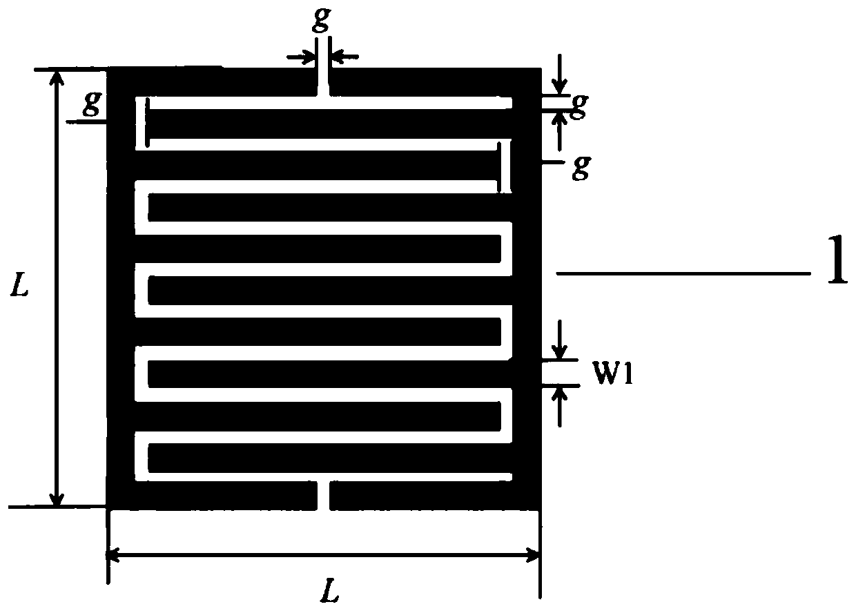
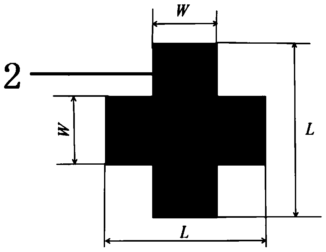
[0028] In this embodiment, the average side length of the upper fork finger structure unit 1 and the lower fork finger structure unit 3 is 6mm, the interfinger gap is 0.204mm, the finger width of the fork finger is 0.36mm, and the length of the fork finger is 5.006mm; The length of each protruding part in the structural unit 2 is 6 mm, the width is 2.4 mm, the thickness of the upper PCB board 4 and the thickness of the lower PCB board 5 are both 2 mm, and the dielectric constant is 3.2 mm. Figure 5 and Image 6 In order to simulate the structure, in the simulation results, it is assumed that the number of the upper interdigital structural unit 1, the cross-shaped structural unit 2 and the lower interdigital structural unit 3 is 30, from Figure 5 It can be seen from the simulation results that the resonant frequency of the radome can be as low as about 2500MHz, and the unit size is only equal to λ 0 / 20, lambda 0 is the free-space wavelength of the resonant frequency electr...


PUM


Abstract

The invention discloses an antenna housing based on a wide-stop-band low-frequency multilayer frequency selective surface. An upper conductive layer is arranged on the upper surface of an upper-layerPCB; a middle conductive layer is arranged on the lower surface of the upper-layer PCB; a lower conductive layer is arranged on the lower surface of a lower-layer PCB; the upper conductive layer is composed of a plurality of upper interdigital structure units which are periodically arranged, the middle conductive layer is composed of a plurality of cross-shaped structure units which are periodically arranged, the lower conductive layer is composed of a plurality of lower interdigital structure units which are periodically arranged, and each upper interdigital structure unit corresponds to onecross-shaped structure unit and one lower interdigital structure unit; each of the upper interdigital structure unit and the lower interdigital structure unit is composed of two comb tooth structures,the lengths of outermost teeth of the two comb tooth structures are the same, the outermost teeth are oppositely distributed, and a gap is formed between the outermost teeth of the two comb tooth structures; each upper interdigital structure unit is completely aligned with the corresponding cross-shaped structure unit and the corresponding lower interdigital structure unit; and the antenna housing has relatively low resonant frequency.

Description

technical field [0001] The invention belongs to the field of electromagnetic engineering and relates to a radome based on a wide stop band low frequency multilayer frequency selective surface. Background technique [0002] At present, for low-frequency (400MHz-3GHz) mobile communication, electronic countermeasures, radar and other electronic equipment, the frequency selection surface radome has narrow bandwidth, narrow stop band, high frequency, harmonics are closer to the fundamental frequency, and the unit is smaller. Large and other problems, there is a greater difficulty in development. The reason is that the sub-wavelength of the low-frequency unit is longer than that of the high-frequency sub-wavelength unit; the structural size of the frequency selective surface unit is much larger when working at low frequencies; the radome often uses many units to simulate infinite periodic structures, which will As a result, the size of the entire radome is too large, resulting in...

Claims


Application Information

Patent Timeline
Patent Type & Authority Applications(China)
IPC IPC(8): H01Q1/42H01Q15/00
CPCH01Q1/42H01Q15/0026
Inventor 郑光明
Owner XIAN UNIV OF POSTS & TELECOMM
Why Eureka
Try Eureka