

Dual-mode bi-pass filter based on capacitance loading square resonant rings
A dual-pass band filter, dual-mode dual-pass technology, applied in resonators, waveguide devices, circuits, etc., can solve the problems of unsatisfactory frequency selectivity, difficult control of filter cavity coupling and external coupling, and achieve Overcome the effect of excessive external coupling coefficient, eliminate mutual interference, and enlarge the feeding coupling area
- Summary
- Abstract
- Description
- Claims
- Application Information
AI Technical Summary
Problems solved by technology
Method used
Image

Examples
Embodiment 1
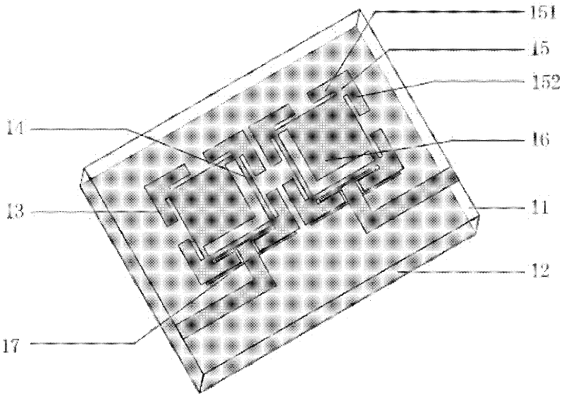
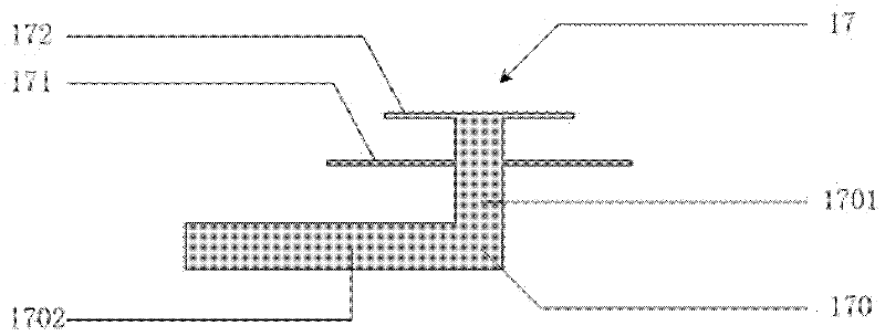
[0042] refer to figure 1 , the present invention is mainly composed of a microstrip dielectric substrate 11, two identical capacitance-loaded square resonant rings 13 and a pair of input and output "dry" type feeders 17. in:
[0043] The lower layer of the microstrip dielectric substrate 11 is a copper-clad grounding plate 12. Two identical capacitance-loaded square resonant rings 13 are located on the upper layer of the microstrip dielectric substrate 11. Each capacitance-loaded square resonant ring 13 is loaded by a square metal ring 14, four The metal sheet 15 is composed of a square perturbation metal sheet 16, the perturbation metal sheet 16 is located inside the square metal ring 14, and the four loading metal sheets 15 adopt an arrow-shaped structure, and the two edges 151 and 152 of the arrow are perpendicular to each other, respectively The two sides of the square metal ring 14 are parallel, and the four loaded metal sheets 15 are respectively located on the four cor...
Embodiment 2
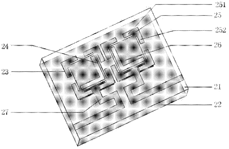
[0047] refer to image 3 , the present invention is mainly composed of a microstrip dielectric substrate 21, two identical capacitance-loaded square resonant rings 23 and a pair of input and output "dry" type feeders 27. in:
[0048] The lower layer of the microstrip dielectric substrate 21 is a copper-clad ground plane 22. Two identical capacitance-loaded square resonant rings 23 are located on the upper layer of the microstrip dielectric substrate 21. Each capacitance-loaded square resonant ring 23 is loaded by a square metal ring 24, four The metal sheet 25 and the square perturbation metal sheet 26 are composed, the perturbation metal sheet 26 is located inside the square metal ring 24, and the four loading metal sheets 25 adopt an arrow-shaped structure, and the two edges 251 and 252 of the arrow are perpendicular to each other, respectively The two sides of the square metal ring 24 are parallel, and the four loaded metal sheets 25 are respectively located on the four co...
Embodiment 3
[0052] refer to Figure 5 , the present invention is mainly composed of a microstrip dielectric substrate 31, two identical capacitance-loaded square resonant rings 33 and a pair of input and output coplanar waveguide feeders 37. in:
[0053] The lower layer of the microstrip dielectric substrate 31 is a copper-clad ground plane 32, and two identical capacitance-loaded square resonance rings 33 are located on the upper layer of the microstrip dielectric substrate 31, and each capacitance-loaded square resonance ring 33 is composed of a square metal ring 34, four The loading metal sheet 35 is composed of a square perturbation metal sheet 36, the perturbation metal sheet 36 is located inside the square metal ring 34, and the four loading metal sheets 35 adopt an arrow-shaped structure and are respectively located on the four corners of the square metal ring 34, These four loaded metal sheets act as capacitors, which can effectively reduce the resonance frequency and reduce the ...
PUM
| Property | Measurement | Unit |
|---|---|---|
| Size | aaaaa | aaaaa |
| Size | aaaaa | aaaaa |
| Size | aaaaa | aaaaa |
Abstract
Description
Claims
Application Information