


Quick Research
Generate reliable direction feasibility study reports for your R&D in just a few steps.

Technical Q&A
Discover and master advanced knowledge NOW. Basics, ideas, possibilities, all at once.

Find Solutions
As an expert in R&D theories, this can generate solutions to your technical problems instantly.

Evaluate Feasibility
Analyze your overall solution with one click, know your potential R&D risks in advance.

Monitor Landscape
Get weekly tech updates, stay abreast of the latest tech innovations and key insights.
Forward-flyback switching power supply circuit
A switching power supply circuit, flyback technology, applied in the direction of high-efficiency power electronic conversion, electrical components, adjusting electrical variables, etc., can solve the problems of low output voltage, increased loss of primary switching tubes, etc., achieve simple circuit, and suppress current mutation , Reduce the effect of current stress and transient voltage stress
- Summary
- Abstract
- Description
- Claims
- Application Information
AI Technical Summary
Problems solved by technology
Method used
Image

Examples
no. 1 example
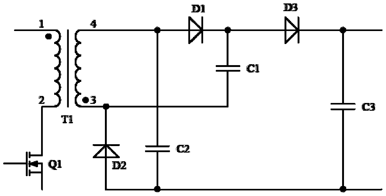
[0038] figure 2 It shows the principle diagram of the first embodiment of the forward and flyback switching power supply circuit of the present invention, including the primary side circuit, the transformer T1 and the secondary side circuit, the primary side circuit includes the switching tube Q1, and the drain of the switching tube Q1 is connected to the 2 terminals of the transformer T1 terminal, the source of the switch tube Q1 is grounded; the secondary circuit includes diode D1, diode D2, diode D3, capacitor C1, capacitor C2, capacitor C3, and inductor L2; terminal 1 and terminal 3 of the transformer T1 are terminals with the same name, and the transformer T1 The 4 ends of the diode D1 are connected to the anode of the diode D1 and one end of the capacitor C2, the other end of the capacitor C2 is connected to the anode of the diode D2 and the other end of the capacitor C3, the cathode of the diode D2 is connected to the 3 ends of the transformer T1 and one end of the indu...
no. 2 example
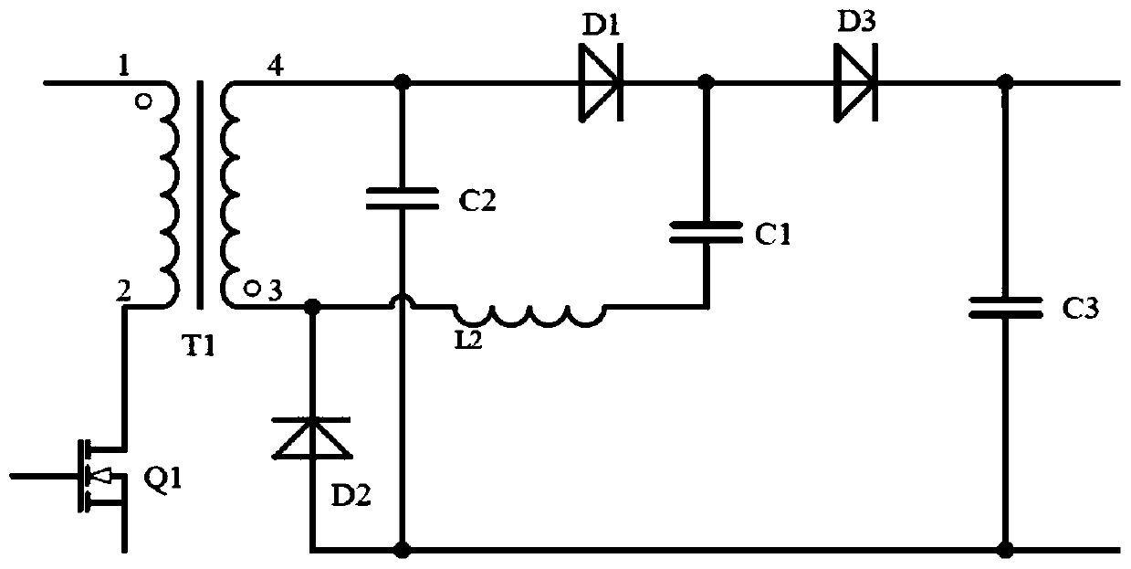
[0043] image 3 It shows the schematic diagram of the second embodiment of the forward and flyback switching power supply circuit of the present invention. The difference from the first embodiment is that the series position of the inductance L2 of the second embodiment is changed to between the diode D1 and the capacitor C1, and the position of the inductance L2 One end is connected to the cathode of the diode D1, and the other end of the inductor L2 is connected to one end of the capacitor C1.
[0044] The working principle of this embodiment is the same as that of the first embodiment, and will not be repeated here.
no. 3 example
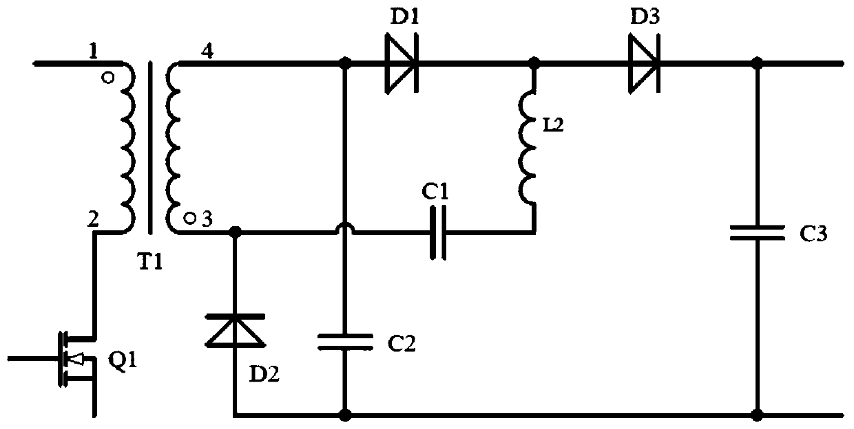
[0046] Figure 4 It shows the schematic diagram of the third embodiment of the forward and flyback switching power supply circuit of the present invention. The difference from the first embodiment is that the series position of the inductance L2 of the third embodiment is changed to between the diode D2 and the capacitor C2, and the position of the inductance L2 One end is connected to the other end of the capacitor C2, and the other end of the inductor L2 is connected to the anode of the diode D2.
[0047] The working principle of this embodiment is the same as that of the first embodiment, and will not be repeated here.
PUM
 Abstract
Description
Claims
Application Information
 - R&D Engineer
- R&D Manager
- IP Professional
- Industry Leading Data Capabilities
- Powerful AI technology
- Patent DNA Extraction
Browse by: Latest US Patents, China's latest patents, Technical Efficacy Thesaurus, Application Domain, Technology Topic, Popular Technical Reports.
© 2024 PatSnap. All rights reserved.Legal|Privacy policy|Modern Slavery Act Transparency Statement|Sitemap|About US| Contact US: help@patsnap.com