Packaging structure of optical module and packaging method thereof

A technology of optical modules and packaging methods, which is applied in the field of optical modules, can solve the problems of high difficulty in mounting cover processing, high development costs of special-shaped molds, and long development cycles, so as to avoid difficult production, reduce packaging costs, and reduce The effect of mold opening cost

Active Publication Date: 2020-04-14
QINGDAO GOERTEK INTELLIGENT SENSOR CO LTD
View PDF4 Cites 5 Cited by
  • Summary
  • Abstract
  • Description
  • Claims
  • Application Information

AI Technical Summary

Problems solved by technology

[0004] The main purpose of the present invention is to provide a packaging structure of an optical module and its packaging method, aiming to solve the problems of high development cost of special-shaped molds, long development cycle, difficulty in mounting cover processing and many defects in the packaging method in the related art. question

Method used


Image

  • Packaging structure of optical module and packaging method thereof
  • Packaging structure of optical module and packaging method thereof
  • Packaging structure of optical module and packaging method thereof

Examples


Embodiment Construction

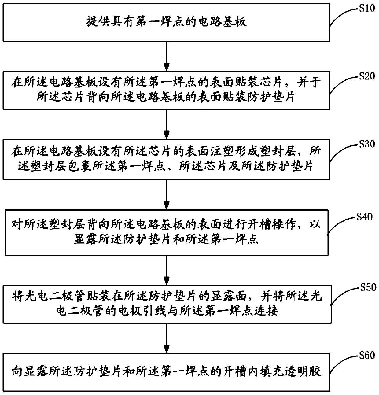
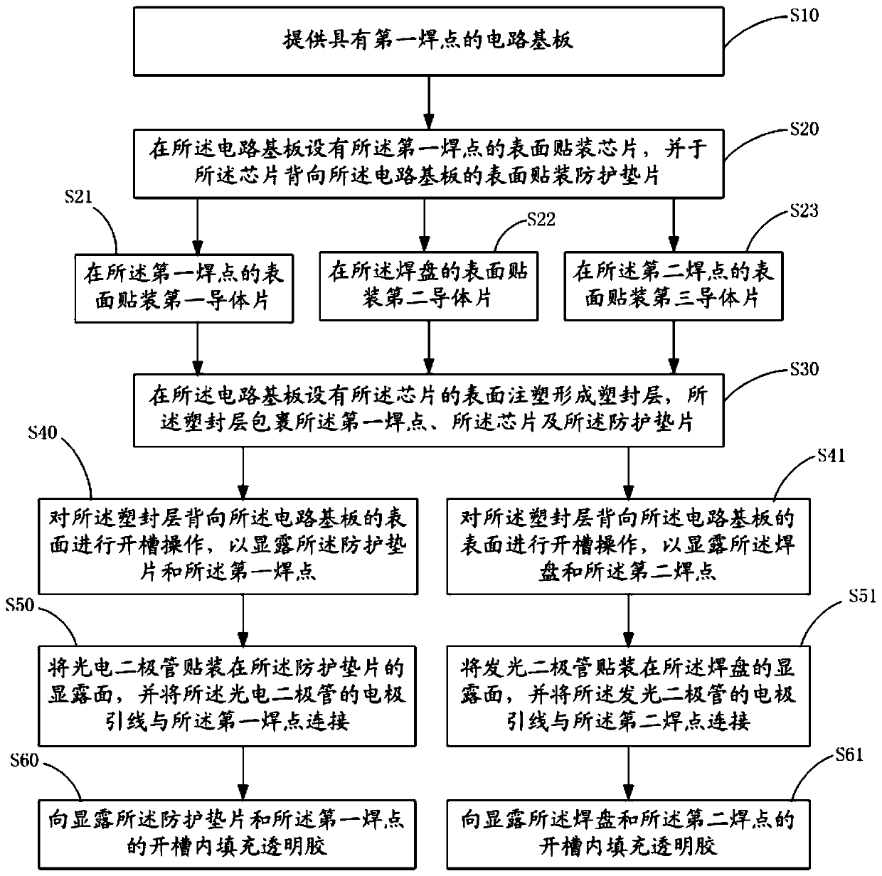
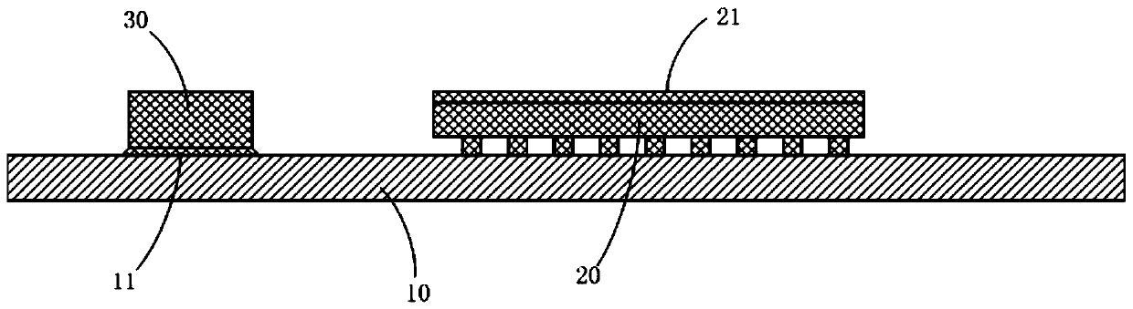
[0041] The following will clearly and completely describe the technical solutions in the embodiments of the present invention with reference to the accompanying drawings in the embodiments of the present invention. Obviously, the described embodiments are only part of the embodiments of the present invention, not all of them. Based on the embodiments of the present invention, all other embodiments obtained by persons of ordinary skill in the art without creative efforts fall within the protection scope of the present invention.

[0042] It should be noted that all directional indications (such as up, down, left, right, front, back...) in the embodiments of the present invention are only used to explain the relationship between the components in a certain posture (as shown in the accompanying drawings). Relative positional relationship, movement conditions, etc., if the specific posture changes, the directional indication will also change accordingly.

[0043] In addition, in t...


PUM


Abstract

The invention discloses a packaging structure of an optical module and a packaging method thereof. The packaging method of the optical module comprises the following steps: providing a circuit substrate with a first welding spot; mounting a chip on the surface, provided with the first welding spots, of the circuit substrate, and mounting a protective gasket on the surface, back to the circuit substrate, of the chip; forming a plastic package layer on the surface, provided with the chip, of the circuit substrate in an injection molding mode, and the plastic package layer wraps the first weldingspots, the chip and the protective gasket; slotting the surface, back to the circuit substrate, of the plastic package layer so as to expose the protective gasket and the first welding spot; and mounting a photodiode on the exposed surface of the protective gasket, and connecting an electrode lead of the photodiode with the first welding spot. According to the technical scheme of the invention, the problems of high development cost, long development period, high processing difficulty of the surface-mounted cover and many defects of a special-shaped mold in a packaging method in the prior artare solved.

Description

technical field [0001] The invention relates to the technical field of optical modules, in particular to an optical module packaging structure and a packaging method thereof. Background technique [0002] In related technologies, the packaging methods of optical modules mainly include encapsulating chips with special-shaped molds and encapsulating chips with mounting lids. These packaging methods often have the following problems: the development cost of special-shaped molds is high, and the development cycle is long; the processing of mounting lids is difficult. Big and flawed. [0003] The above content is only used to assist in understanding the technical solution of the present invention, and does not mean that the above content is admitted as prior art. Contents of the invention [0004] The main purpose of the present invention is to provide an optical module packaging structure and its packaging method, which aims to solve the problems of high development cost of s...

Claims


Application Information

Patent Timeline
Patent Type & Authority Applications(China)
IPC IPC(8): H01L21/56H01L23/31H01L25/16
CPCH01L21/56H01L23/3114H01L23/3121H01L23/3135H01L23/3142H01L25/167
Inventor 王伟王文涛宋其超孙艳美孙恺汪奎
Owner QINGDAO GOERTEK INTELLIGENT SENSOR CO LTD
Why Eureka
Try Eureka