Manufacturing method for low-cost monocrystalline silicon chips for photovoltaic cells

A cost-effective single-crystal, photovoltaic cell technology, applied in fine working devices, manufacturing tools, stone processing equipment, etc., can solve problems such as increasing production costs, consuming a large amount of electricity, increasing the consumption of carbon footprint of single-crystal silicon wafers, etc. Carbon footprint, effect of reducing overall electricity consumption

Inactive Publication Date: 2020-04-21
江苏美科太阳能科技股份有限公司 +1
View PDF5 Cites 10 Cited by
  • Summary
  • Abstract
  • Description
  • Claims
  • Application Information

AI Technical Summary

Problems solved by technology

[0005] The drawing of single-crystal wafers needs to consume a lot of electric energy, inert gas, thermal field composed of high-purity graphite materials, furnace equipment, etc., resulting in high non-silicon cost of round rods (or single-crystal silicon wafers), accounting for the current cost of single-crystal silicon wafers. About 25% of
30%-40% of the edge leather is not used in the production of silicon wafers, which not only increases the production cost, but also increases the carbon footprint consumption of monocrystalline silicon wafers, which is not conducive to environmental protection

Method used


Image

  • Manufacturing method for low-cost monocrystalline silicon chips for photovoltaic cells
  • Manufacturing method for low-cost monocrystalline silicon chips for photovoltaic cells

Examples


Embodiment Construction

[0024] A method for manufacturing a low-cost monocrystalline silicon wafer for photovoltaic cells provided in this embodiment includes

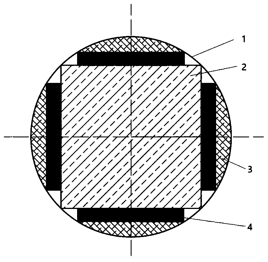
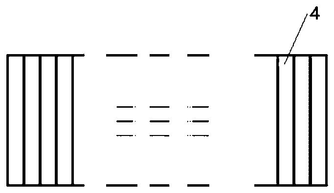
[0025] S1. Cut off a single wafer rod 1 with a length of 650 mm and a diameter of 300 mm, such as figure 1 As shown, the square is divided into two steps: first, set the square line according to the spacing of 210+20+20mm, cut the 300mm round bar 1 into a quasi-square bar 2 with a side length of 250mm, and produce 4 pieces of round arches Material 3; then this quasi-square bar 2 is cut into a square bar with a side length of 210mm, and four monocrystalline slabs 4 with a thickness of 20mm and a length of 650mm are produced;

[0026] S2. Bonding a certain number of single crystal slabs 4 together with hydrosol, and using a polycrystalline squarer to square the single crystal slabs 4 into a silicon block with a size of 158mmx158mm and a thickness of 20mm;

[0027] S3. Bond the silicon blocks together with hydrosol to form a composite square ro...


PUM


Abstract

The invention discloses a manufacturing method for low-cost monocrystalline silicon chips for photovoltaic cells, and relates to the technical field of monocrystalline silicon chip manufacturing. Thesilicon chips produced by the method are cut from original waste monocrystalline flaw-pieces and has no crystal production cost; the cost of each produced silicon chip is reduced by 0.7 yuan and the selling price can be reduced by more than 20%, so that the silicon chips are tangible low-cost silicon chips.

Description

technical field [0001] The invention relates to the technical field of monocrystalline silicon wafer manufacturing, in particular to a method for manufacturing a low-cost monocrystalline silicon wafer used for photovoltaic cells. Background technique [0002] With the large-scale application of diamond wire slicing and the application of high-efficiency cell technologies such as PERC and HIT, monocrystalline silicon wafers have gradually become the main substrate material for photovoltaic cells due to their advantages such as less defects, high carrier life, and stable quality. [0003] At present, single crystal silicon wafers used in photovoltaic cells are cut into squares by pulling single wafer rods and then cut with diamond wires. The edge material produced by cutting the round rod into squares is reused as a recycled material after cleaning. The use of crystals (square rods or quasi-square rods) for cutting silicon wafers accounts for only 60%-70%, that is, 30%- 40% o...

Claims


Application Information

Patent Timeline
IPC IPC(8): B28D5/04
CPCB28D5/045
Inventor 张志强王艺澄周炎姚亮
Owner 江苏美科太阳能科技股份有限公司
Why Eureka
Try Eureka