Supercharge Your Innovation With Domain-Expert AI Agents!

Display panel and preparation method thereof

A display panel and display area technology, applied in semiconductor/solid-state device manufacturing, electrical components, electric solid-state devices, etc., can solve the problems of reducing impact, sacrificing bending performance, and reducing yield, so as to achieve reduced reflection and excellent pixel electrodes pattern effect

Inactive Publication Date: 2020-04-21
SHENZHEN CHINA STAR OPTOELECTRONICS SEMICON DISPLAY TECH CO LTD
View PDF2 Cites 5 Cited by
  • Summary
  • Abstract
  • Description
  • Claims
  • Application Information

AI Technical Summary

Problems solved by technology

[0003] Due to the low luminous efficiency of OLEDs at present, it is generally difficult to obtain high enough brightness to obtain high contrast effects under strong external light under the consideration of power consumption balance. Due to the existence of external light reflection, OLEDs When displaying, the human eye receives the influence of reflected light, which interferes with the actual display effect of OLED
At present, methods such as additional circular polarizers are usually used to prevent the incident light from re-exiting and reduce the impact
However, the use of additional polarizers, on the one hand, increases the thickness of the screen and sacrifices the bending performance. On the other hand, the introduction of additional process steps increases the cost and reduces the yield.

Method used


Image

  • Display panel and preparation method thereof
  • Display panel and preparation method thereof
  • Display panel and preparation method thereof

Examples


Embodiment Construction

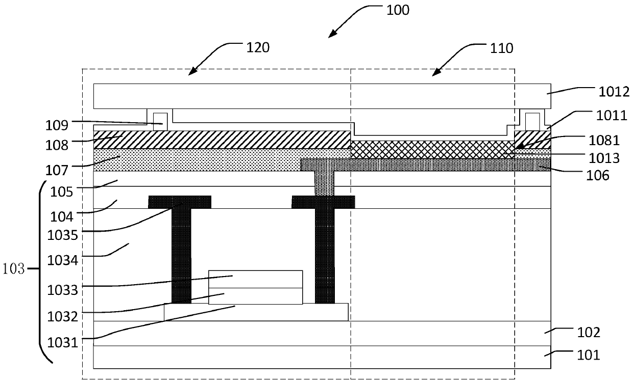
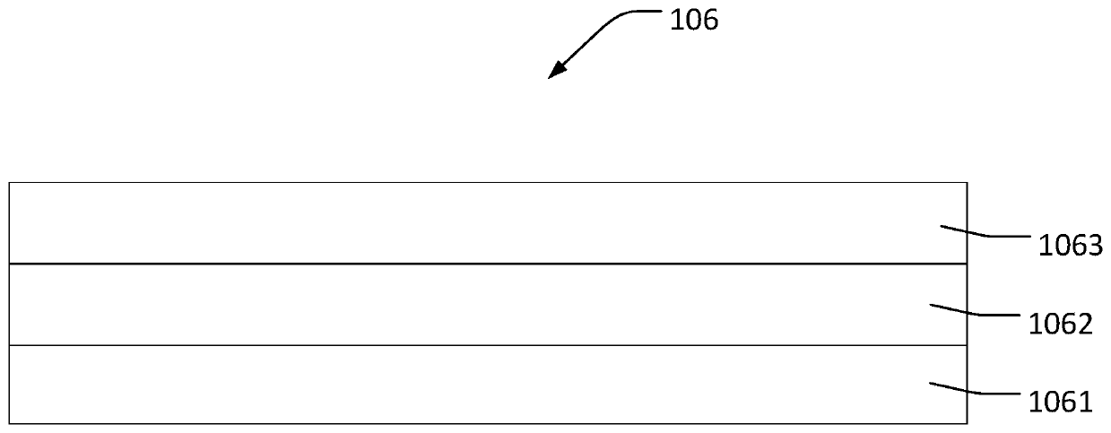
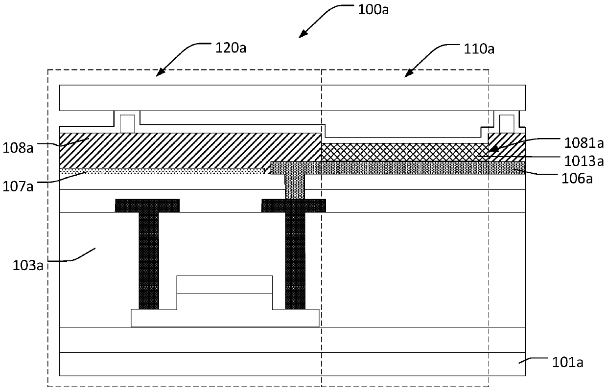
[0034] The following description of various embodiments is made with reference to the accompanying drawings to illustrate specific embodiments in which the invention may be practiced. The directional terms mentioned in the present invention, such as up, down, front, back, left, right, inside, outside, side, etc., are only directions referring to the drawings. The component names mentioned in the present invention, such as first, second, etc., are only used to distinguish different components, which can be better expressed. In the figures, structurally similar elements are denoted by the same reference numerals.

[0035] Embodiments of the present invention will be described in detail herein with reference to the accompanying drawings. This invention may be embodied in many different forms and should not be construed as only the specific embodiments set forth herein. These embodiments are provided to explain the practical application of the invention, so that others skilled i...


PUM


Abstract

The invention provides a display panel and a preparation method thereof. The reflection of external light on a display is reduced by manufacturing an amorphous silicon film layer for absorbing visiblelight, the light absorption layer is preferably disposed on a first electrode, a mask is formed by utilizing the inherent pattern of a pixel definition layer, that is, a through hole is formed in a light-emitting area of the pixel definition layer, and the through hole penetrates through the light absorption layer, so that the first electrode is exposed in the through hole, the first electrode exposed in the through hole is an effective electrode, the through hole removes the light absorption layer in a display area, and the light absorption layer only exists in a non-display area. Therefore,the effective first electrode structure does not have an overlapping region with the light absorption layer, so that an excellent pixel electrode pattern and the light absorption layer completely covering the non-light-emitting area can be combined.

Description

technical field [0001] The invention relates to the display field, in particular to a display panel and a preparation method thereof. Background technique [0002] Active matrix organic light emitting diode panel (Organic Light Emitting Diode, OLED) is a display technology that has received widespread attention at present, with many advantages such as self-illumination, high brightness, high contrast, wide viewing angle, fast response, low power consumption, and thinness , known as the next generation display technology. This technology is widely used in electronic terminal products, home appliances, vehicles and other fields. When applied to handheld and other terminal products, due to the possibility of various application scenarios, handheld terminal products put forward higher requirements on the display effect under natural light. [0003] Due to the low luminous efficiency of OLEDs at present, it is generally difficult to obtain high enough brightness to obtain high ...

Claims


Application Information

Patent Timeline
Patent Type & Authority Applications(China)
IPC IPC(8): H01L51/52H01L27/32H01L51/56
CPCH10K59/122H10K59/8792H10K59/1213H10K71/621H10K59/87H10K50/865H10K71/00H10K50/8428H10K59/1201
Inventor 杜彦英
Owner SHENZHEN CHINA STAR OPTOELECTRONICS SEMICON DISPLAY TECH CO LTD
Features
  • R&D
  • Intellectual Property
  • Life Sciences
  • Materials
  • Tech Scout
  • Unparalleled Data Quality
  • Higher Quality Content
  • 60% Fewer Hallucinations
Learn More