A scanning probe processing method for micro-nano structures derived from graphene edges
A scanning probe, micro-nano structure technology, applied in the field of micro-nano processing, can solve the problems of difficult processing paths, difficult to directly process nanostructures, and many processing methods and steps, and achieve economical, flexible, excellent mechanical and The effect of electrical properties
- Summary
- Abstract
- Description
- Claims
- Application Information
AI Technical Summary
Problems solved by technology
Method used
Image
Examples
example 1
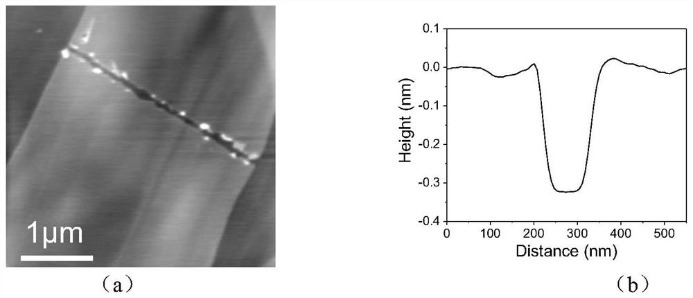
[0026] Adopt the method of the present invention to process the nano channel, the process is as follows:
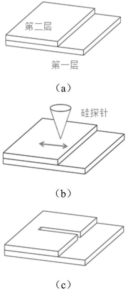
[0027] A1. Install the tapered silicon probe with strong surface chemical activity on the scanning probe processing equipment, then place the prepared graphene sample on the processing table, scan to obtain the graphene surface morphology, and search for the graphene edge.
[0028] A2. Position the scanning probe to the graphene edge area, set its trajectory, and control the probe to scratch from the graphene edge to the inside under the action of low contact pressure (such as normal load 1μN), and observe the friction The change of the force curve monitors the processing status in real time; the specific scanning probe equipment will feed back the friction curve of the interaction between the probe and graphene during the processing process, and the processing status can be judged in real time through the friction curve, as well as the set processing status. Whether the ...
example 2
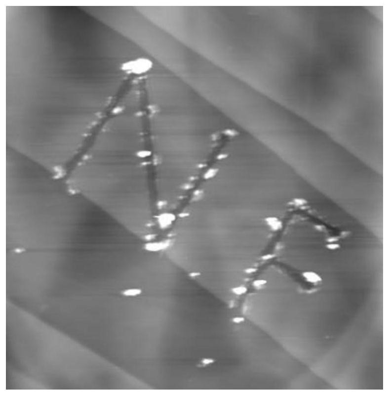
[0032] The micro-nano letter structure processed on the surface of graphene by scanning probe and graphene edge tribochemical processing method, the processing process is as follows:
[0033] B1, the sample preparation steps are the same as in Example 1, first look for the graphene atomic step edge;
[0034] B2. Position the scanning probe to the edge of the graphene step, set the load for processing letters and the trajectory of the probe, and control the probe to carve and process the micro-nano letter structure along the trajectory;
[0035] B3. After the processing is completed, the micro-nano letter structure morphology of the processing area is obtained by in-situ scanning.
[0036] image 3 In order to use the method of this example to process the letter combination "NF", which is the abbreviation of "Nano-Fabrication".
[0037] The probe material with strong surface chemical activity in the present invention is one of silicon, silicon dioxide, ceria, and silicon nitr...
PUM
 Abstract
Description
Claims
Application Information


