Circuit board buried hole resin hole plugging method

A resin plug hole, circuit board technology, applied in printed circuit, multilayer circuit manufacturing, printed circuit manufacturing and other directions, can solve production problems, thin plate grinding plate expansion and shrinkage, serious problems, achieve good reliability, solve the problem of cracked board , to avoid the effect of expansion and contraction problems

Pending Publication Date: 2020-05-01
东莞市五株电子科技有限公司
View PDF9 Cites 6 Cited by
  • Summary
  • Abstract
  • Description
  • Claims
  • Application Information

AI Technical Summary

Problems solved by technology

However, in practical application, it is found that after the buried hole resin plug hole is solidified, the grinding process cannot be carried out due to the thinness of the plate, and the expansion and shrinkage of the thin plate grinding plate is more serious, causing great troubles to production

Method used


Image

  • Circuit board buried hole resin hole plugging method
  • Circuit board buried hole resin hole plugging method

Examples


Embodiment 1

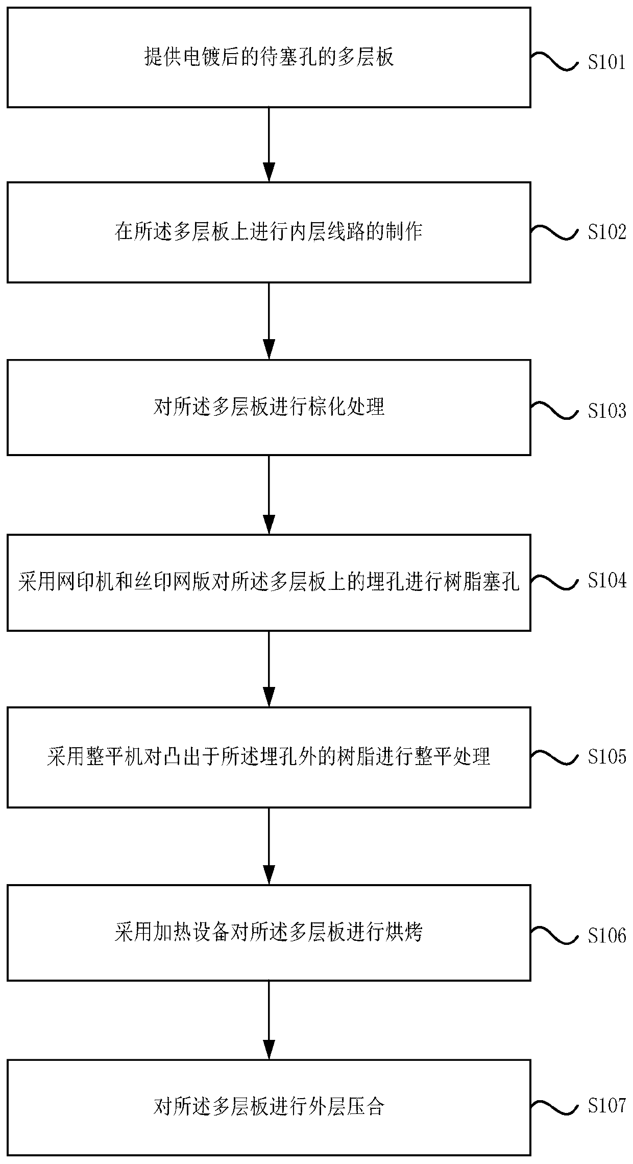
[0039] Please refer to the attached figure 1 , is a schematic flow chart of a method for resin plugging buried holes in circuit boards provided by Embodiment 1 of the present invention. This method is applicable to the scene of performing resin plugging on buried holes of HDI boards whose board thickness is getting thinner and thinner. The method specifically includes the following steps:

[0040] S101, providing a multi-layer board with holes to be plugged after electroplating;

[0041] Specifically, before the step S101, the method further includes:

[0042] (1) Pressing the prepared inner layer core board and the prepreg to obtain a multi-layer board;

[0043] (2) drilling the multi-layer board to form buried holes;

[0044] (3) Perform electroplating treatment on the multi-layer board.

[0045] S102. Fabricate inner-layer circuits on the multi-layer board;

[0046] S103, performing browning treatment on the multi-layer board;

[0047] It should be noted that the purp...


PUM

PropertyMeasurementUnit
thicknessaaaaaaaaaa
pore sizeaaaaaaaaaa

Abstract

The invention discloses a circuit board buried hole resin hole plugging method. The method comprises the following steps of: providing an electroboardd multilayer board to be subjected to hole plugging, manufacturing an inner layer circuit on the multilayer board, carrying out browning treatment on the multilayer board, performing resin hole plugging on the buried holes in the multilayer board byadopting a screen printer and a screen printing board, conducting leveling treatment on the resin protruding out of the buried hole through a leveling machine, baking the multilayer board by adoptingheating equipment, and laminating the outer layer of the multilayer board. According to the circuit board buried hole resin hole plugging method provided by the invention, through the process technology of resin hole plugging after browning, the trouble of thin board resin board grinding in the prior art is solved, the expansion and shrinkage problems caused by thin board resin hole plugging boardgrinding are avoided, on the other hand, the board explosion problem caused by thin PP pressing glue filling shortage is solved, and good reliability of products is guaranteed.

Description

technical field [0001] The invention relates to the technical field of circuit board manufacturing, in particular to a method for resin plugging holes in circuit boards. Background technique [0002] HDI (High Density Interconnector) board, that is, high-density interconnect board, is a circuit board with relatively high circuit distribution density using micro-blind buried hole technology. The HDI board has an inner layer circuit and an outer layer circuit, and then uses processes such as drilling and metallization in the hole to realize the internal connection of each layer of circuits. [0003] At present, the thickness of the high-end HDI board is getting thinner and thinner. After the first lamination, the thickness of the board is about 0.40mm, and the number of buried holes may reach 140,000 holes / pnl, corresponding to the second lamination PP (Prepreg Prepreg) is thin PP such as 106 or 1037. The existing process of resin plugging hole buried hole in HDI board is: b...

Claims


Application Information

Patent Timeline
Patent Type & Authority Applications(China)
IPC IPC(8): H05K3/00H05K3/46
CPCH05K3/0014H05K3/0094H05K3/46H05K2203/1105
Inventor 孟昭光赵南清蔡志浩曾国权
Owner 东莞市五株电子科技有限公司
Why Eureka
Try Eureka