

Optical coupler and manufacturing method thereof
An optical coupler and optical detection technology, which is applied in the coupling of optical waveguides, optical guides, optics, etc., can solve the problems of increased input power consumption of the device, the area of the photodiode should not be too large, and the output current capability of the photodiode is weak.
- Summary
- Abstract
- Description
- Claims
- Application Information
AI Technical Summary
Problems solved by technology
Method used
Image

Examples
Embodiment Construction
[0024] In order to illustrate the present invention more clearly, the present invention will be further described below in conjunction with preferred embodiments and accompanying drawings. Similar parts in the figures are denoted by the same reference numerals. Those skilled in the art should understand that the content specifically described below is illustrative rather than restrictive, and should not limit the protection scope of the present invention.
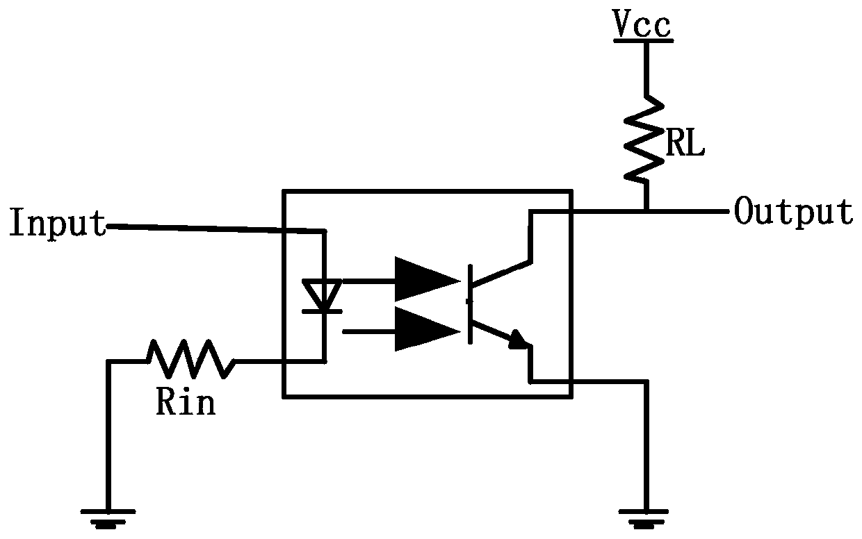
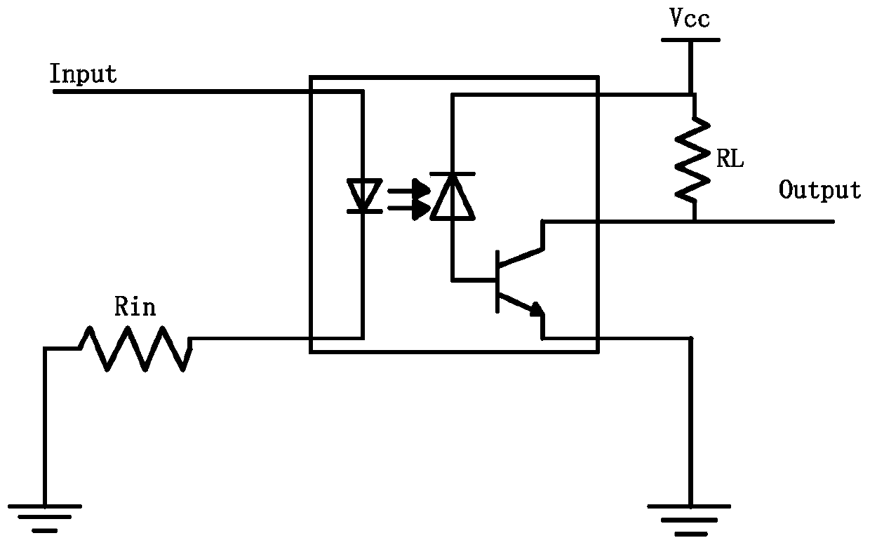
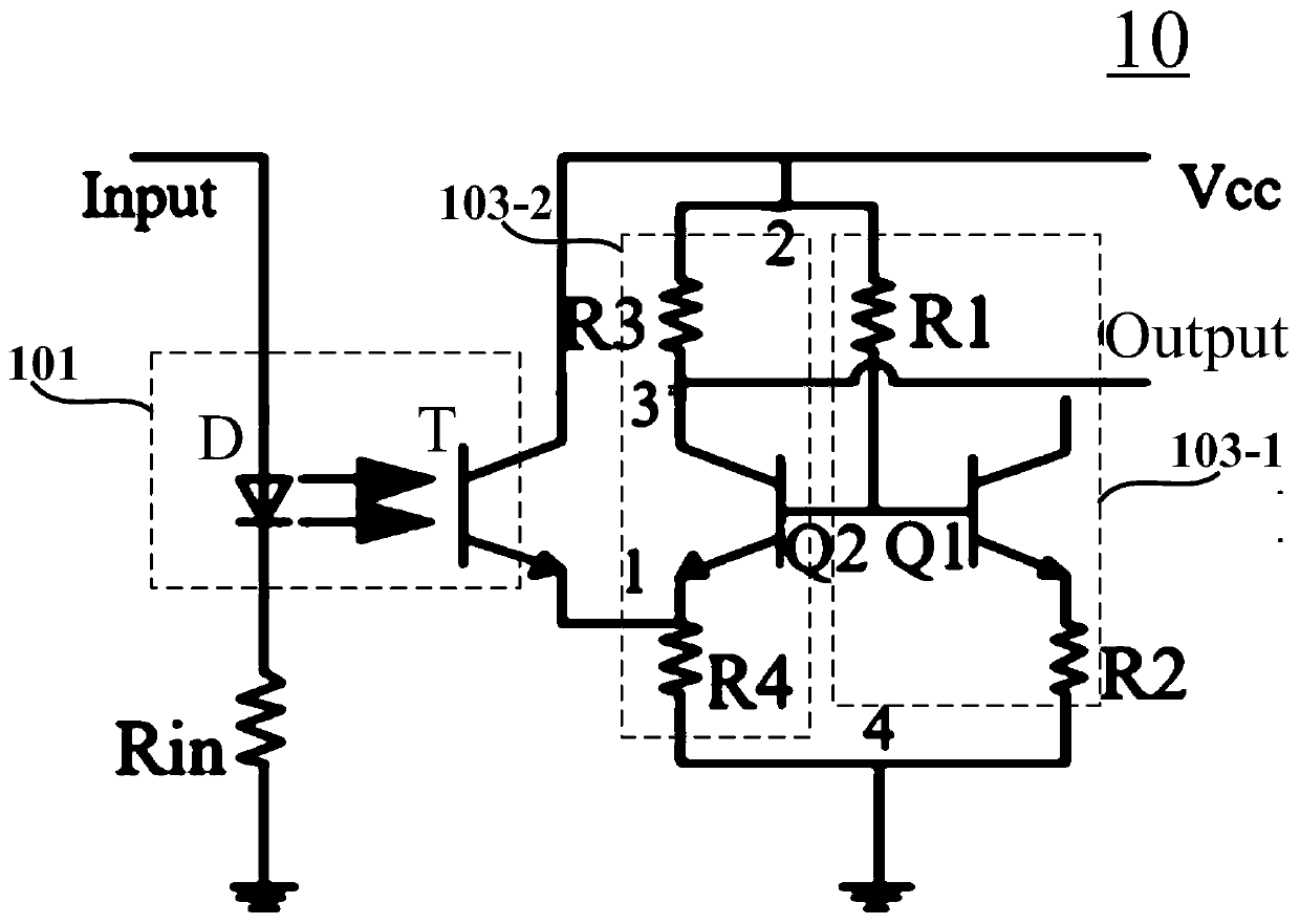
[0025] Combine below image 3 with Figure 4 Describe the structural principle of the optical coupler 10 according to the embodiment of the present application, wherein, image 3 It is a schematic circuit schematic diagram of an optocoupler 10 according to an embodiment of the present application; Figure 4 It is a schematic diagram showing each port of the optical coupler 10 according to the embodiment of the present application.
[0026] combine first image 3 Describe the specific internal structure of the circuit. ...
PUM
 Abstract
Description
Claims
Application Information