Display panel, manufacturing method thereof and display device

A display panel and flexible display technology, applied in the fields of display devices, display panels and manufacturing methods thereof, can solve the problems of weak impact resistance, source-drain metal wire breakage, etc., and achieve the effect of being less prone to breakage

Active Publication Date: 2020-05-08
BOE TECH GRP CO LTD +1
9 Cites 15 Cited by

AI-Extracted Technical Summary

Problems solved by technology

[0004] The purpose of the present invention is to provide a display panel and its manufacturing method, display device, to solve the weak ...

Method used

Please further refer to Fig. 1, in some embodiments, one end of colloid 20 is set to circular arc shape, and the end of this circular arc is corresponding to the shape matching of bending zone 13, thus the circular arc end of colloid 20 The part is attached and fixed to the inner surface of the bending area 13, so as to further improve the supporting effect of the colloid 20 on the second arcuate area 14.
Please further refer to Fig. 1, in some embodiments, the outside of bending area 13 is coated with the 3rd colloid 19, and the 3rd colloid 19 is arranged at least on the side surface of bending area 13 away from colloid 20, uses In the protection bending zone 13. The third colloid 19 is an ultraviolet curable glue to prevent the source and drain metal wires in the bending area 13 from breaking.
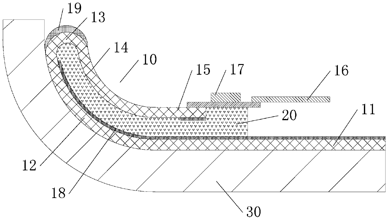
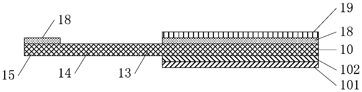
[0041] An embodiment of the present invention provides a display panel, as shown in FIG. 1 , including a flexible display substrate 10 and a colloid 20. The flexible display substrate 10 includes a plane area 11, a first arc area 12, a bending area 13, a second arc area 14 and an edge area 15, the plane area 11 and the first arc area 12 are display areas, and the second arc area The area 14 corresponds to the shape matching of the first arcuate area 12 . The second arc-shaped area 14 and the edge 15 are located on the back side of the display area after being bent by the bending area 13, so that the edge area 15 connecting the pixel lead line to the external circuit is located on the back side of the display area, realizing the narrow frame of the curved display screen Effect. After the flexible display substrate 10 is bent, the planar area 11, the first arc area 12, the bending area 13, the second arc area 14 and the edge area 15 are enclosed to form an accommodation space, in order to avoid the second arc after bending Shaped area 14 appears suspended state, the present invention fills colloid 20 in accommodating space, and colloid 20 is bonded and fixed with second arc-shaped area 14, edge area 15 and first arc-shaped area 12, planar area 11, and colloid 20 also The second arc region 14 is supported to prevent the impact resistance of the display panel from being reduced due to the suspended state of the s...

Abstract

The invention discloses a display panel. The display panel comprises a flexible display substrate and colloid, the flexible display substrate comprises a plane area, a first arc-shaped area, a bendingarea, a second arc-shaped area and an edge area which are connected in sequence. The shapes of the first arc-shaped area and the second arc-shaped area are matched and correspond to each other; wherein the plane area, the first arc-shaped area, the bending area, the second arc-shaped area and the edge area define a containing space, the containing space is filled with the colloid to support the second arc-shaped area, and the plane area, the first arc-shaped area, the second arc-shaped area and the edge area are bonded and fixed through the colloid. The colloid is used for filling the containing space, the situation that the impact resistance of the display panel is reduced due to the fact that the second arc-shaped area is in a suspended state is avoided, and the source-drain metal wiresin the bent area are not prone to breakage.

Application Domain

Technology Topic

Image

  • Display panel, manufacturing method thereof and display device
  • Display panel, manufacturing method thereof and display device
  • Display panel, manufacturing method thereof and display device

Examples

  • Experimental program(1)

Example Embodiment

[0039] In order to illustrate the present invention more clearly, the present invention will be further described below with reference to the preferred embodiments and accompanying drawings. Similar parts in the figures are denoted by the same reference numerals. Those skilled in the art should understand that the content specifically described below is illustrative rather than restrictive, and should not limit the protection scope of the present invention.
[0040] The thickness of each layer, the size and shape of the region in the accompanying drawings do not reflect the actual proportion of each layer, and the purpose is only to illustrate the content of the present invention.
[0041] Embodiments of the present invention provide a display panel, such as figure 1 As shown, the flexible display substrate 10 and the gel 20 are included. The flexible display substrate 10 includes a flat area 11, a first arc area 12, a bending area 13, a second arc area 14 and an edge area 15. The plane area 11 and the first arc area 12 are the display area, and the second arc area The area 14 corresponds to the shape matching of the first arcuate area 12 . The second arc-shaped area 14 and the edge 15 are located on the back side of the display area after being bent by the bending area 13, so that the edge area 15 where the pixel lead lines are connected to the external circuit is located on the back side of the display area, so as to realize the narrow frame of the curved display screen Effect. After the flexible display substrate 10 is bent, the flat area 11 , the first arc area 12 , the bending area 13 , the second arc area 14 and the edge area 15 are enclosed to form an accommodation space. The shape area 14 is in a suspended state, the present invention fills the accommodating space with the colloid 20, the colloid 20 glues and fixes the second arc-shaped area 14 and the edge area 15 with the first arc-shaped area 12 and the plane area 11, and the colloid 20 also The second arc-shaped area 14 is supported to prevent the impact resistance of the display panel from being reduced due to the suspended state of the second arc-shaped area 14 , so that the source-drain metal lines of the bending area 13 are not easily broken.
[0042] In some embodiments, the display area of ​​the flexible display substrate 10 can display a picture, and the displayed picture can be actually viewed by the user.
[0043] In some embodiments, edge region 15 includes traces and the like. On this basis, the edge region 15 may further include a gate driving circuit.
[0044] In some embodiments, the second arc region 14 and the edge region 15 of the flexible display substrate 10 are bent to the back of the display region, in order to realize a narrow frame design of the flexible display substrate 10 . Wherein, taking the flexible display substrate 10 as a rectangle as an example, one or two or three or four edge regions 15 of the flexible display substrate 10 can be bent to the back of the display region.
[0045] Optionally, the four edge areas 15 of the flexible display substrate 10 are all bent to the back of the main display area, so as to achieve a narrow frame design to the greatest extent and increase the screen ratio.
[0046] In some embodiments, the display substrate 10 further includes a circuit board 16 disposed on the back of the display area. The circuit board 16 may be, for example, a flexible circuit board (Flexible circuit board, FPC for short).
[0047] The driving chip 17 can be mounted on the array substrate of the flexible display substrate 10 by the method of chip on film (COF for short) or the method of chip on panel (COP for short), and the FPC Power is supplied to the driver chip 17 and various signals are provided. Regardless of the COP method or the COF method, the FPC is bent along at least one end of the flexible display substrate 10 to the back of the display area.
[0048]In some embodiments, the flexible display substrate 10 may be, for example, an organic light-emitting diode (Organic Light-Emitting Diode, OLED for short) display substrate, or a light emitting diode (Micro-LED) display substrate, or a quantum Dot electroluminescence (Quantum Dot Light Emitting Diodes, QLED for short) display substrate.
[0049] In some embodiments, the colloid 20 may be one or more layers of polymer materials, such as polyethylene terephthalate (PET), foam tape, acrylic at least one of. The material of the colloid 20 can also be a rubber or plastic material with good film-forming properties. In this case, a certain thickness of PET or acrylic adhesive material needs to be coated on both sides of the colloid 20 to facilitate pasting.
[0050] Please refer to further figure 1 , in some embodiments, one end of the colloid 20 is set as a circular arc, and the end of the circular arc matches the shape of the bending area 13 , so that the arc-shaped end of the colloid 20 corresponds to the inner side of the bending area 13 The surfaces are attached and fixed, thereby further improving the supporting effect of the colloid 20 on the second arc-shaped area 14 .
[0051] like figure 2 As shown, the surface of the flexible display substrate 10 is provided with an optical film layer 101 and an encapsulation layer 102 for encapsulating the OLED. The optical film layer 101 may be a stack of various optical films, such as polarizer (POL), OCA, touch screen, etc. The back side of the flexible display substrate 10 is provided with a back film 18 and a heat dissipation layer 19 .
[0052] The back film 18 flattens the flexible display substrate, and then processes such as dicing and IC (Integrated Circuit, integrated circuit) chip bonding are performed, and then the back film on the bending region 13 is removed before the bending process. In some embodiments, the width of removing the back film is increased, the back film layer of the bending area 13 and the second arc area 14 is removed, and the back film is only retained on the plane area 11 , the first arc area 12 and the edge area 15 film layer. The heat dissipation layer 19 can improve the heat dissipation effect of the flexible display substrate 10 .
[0053] like image 3 As shown, in order to facilitate the display of the colloid 20, the shape of the colloid 20 in the following figures is a straight line. The surface of the gel 20 is provided with grooves 21 , and the grooves 21 are used for accommodating the back film 18 on the edge area 15 to improve the flatness of the adhesive 20 , the second arc area 14 and the edge area 15 .
[0054] In some embodiments, the groove 21 divides the colloid 20 into a first colloid 22 and a second colloid 23 , the first colloid 22 is close to the bending area 13 , the second colloid 23 is far away from the bending area 13 , the first colloid 22 and the second colloid 23 are separated from each other. The thickness of the colloid 23 may be different, and the thickness of the first colloid 22 is smaller than the thickness of the second colloid 23 . Thickness H of the first colloid 1 by formula H 1 =2R-L is determined, wherein R is the arc radius of the bending region 13 , and L is the thickness of the back film 18 .
[0055] in as Figure 4 In some of the illustrated embodiments, the thicknesses of the first colloid 22 and the second colloid 23 are the same, and the fluidity of the colloid 20 is used to fill the gaps at different thicknesses of the accommodating space.
[0056] in as Figure 5 In some embodiments shown, during the process of removing the back film, all the back films on the bending area 13, the second arc area 14 and the edge area 15 are removed. Under this structure, no grooves are provided on the colloid 20. 21. The colloid 20 can maintain a uniform thickness, or the thickness of the colloid 20 in the edge region 15 is slightly larger than the thickness of the second arc region 14.
[0057] In some embodiments, as Figure 7 The shape of the gel 20 shown is such that when the COP process is used, the gel 20 located in the edge region 15 is provided with a groove 21 , and the groove 21 is used for accommodating the backing film 18 . The colloid 20 can also maintain a uniform thickness, and the fluidity of the colloid 20 can be used to fill the gaps at different thicknesses of the accommodating space. The colloids designed for the COF process and the COP process can also be used interchangeably.
[0058] Please refer to further figure 1 In some embodiments, the outer side of the bending area 13 is coated with a third colloid 19 , and the third colloid 19 is disposed at least on the side surface of the bending area 13 away from the colloid 20 to protect the bending area 13 . The third colloid is a 19-bit ultraviolet curing glue to prevent the source-drain metal lines of the bending region 13 from breaking.
[0059] In some embodiments, the length H of the third colloid 19 2 by formula Determine, where R is the arc radius of the bending area 13, r is the radian of the first arc area, L 1 is the length of the climbing area on one side of the third colloid.
[0060] In some embodiments, a heat dissipation layer 19 is further provided on the flat area 11 of the flexible display substrate 10 and the back film of the first arc area 12 , and the heat dissipation layer is formed by a heat dissipation film for cooling the flexible display substrate 10 by heat dissipation. , to improve the stability of the flexible display substrate 10 .
[0061] An embodiment of the present invention further provides a display device having the above-mentioned display panel.
[0062] Embodiments of the present invention further provide a method for manufacturing the above-mentioned display panel, such as figure 1 and image 3 shown, can be achieved by the following steps:
[0063] A back film 18 is attached to the back surface of the flexible display substrate 10;
[0064] Part of the back film 18 is removed, and the back film 18 is removed by extending toward the edge area 15 from the junction of the bending area 13 and the first arc area 12 as a starting point;
[0065] The flexible display substrate 10 is attached to the cover glass 30, and the cover glass 30 can be curved glass with two sides or four sides, figure 1 Only the curved edge portions of the flexible display substrate 10 and the cover glass 30 are shown in FIG.
[0066] Using the positioning marks on the protective film of the colloid 20 to align and attach the flexible display substrate 10, the colloid 20 is bonded to the plane area 11 and the first arc area 12;
[0067] Use the adsorption head to adsorb FPC16 or COF and bend it along the bending area 13, perform alignment after bending, and bond the second arc area 14 and the edge area 15 to the other side surface of the colloid 20;
[0068] The second arcuate region 14 and the edge region 15 are pressed together using the indenter 40 as shown.
[0069] In the embodiment of the present invention, the colloid 20 is used to fill the accommodating space enclosed by the flat area 11 , the first arc area 12 , the bending area 13 , the second arc area 14 and the edge area 15 after the flexible display substrate 10 is bent. , to prevent the impact resistance of the display panel from being reduced due to the second arc-shaped region 14 being in a suspended state, so that the source-drain metal lines of the bending region 13 are not easily broken.
[0070] like Figure 4 The shown indenter 40 includes a curved area 41 and a straight area 42, and a pressure rod 43 connected to the curved area 41 and the straight area 42. The shape of the curved area 41 is matched with the second arc area 14. 40, the second arc region 14, the edge region 15, the first arc region 12, the plane region 11 and the colloid 20 are firmly bonded.
[0071] In some embodiments, when part of the back film 18 is removed, the width L of the back film 18 is removed 2 by formula Wherein, R is the arc radius of the bending area, R' is the arc radius of the back film of the first arc area, L 3 is the thickness of all film layers below the cover glass, and r' is the curvature of the bent portion of the cover glass.
[0072] Please refer to Figure 5 , In some embodiments, the indenter 40 has a split structure, the arc area 41 and the straight area 42 are separated, and can be moved under the driving of the respective pressing rods 43 . When pressing, you can first use the arc area 41 to press the second arc area 14, and then use the straight area 42 to press the edge area 15, or you can use the straight area 42 to press the edge area 15 first, and then use the arc area to press the edge area 15. The surface area 41 is pressed against the second arc surface area 14 .
[0073] In some embodiments, the downward pressure of the curved surface area 41 and the flat surface area 42 can be adjusted separately, that is, the downward pressure force of the curved surface area 41 and the flat surface area 42 can be the same or different.
[0074] Obviously, the above-mentioned embodiments of the present invention are only examples for clearly illustrating the present invention, and are not intended to limit the embodiments of the present invention. Changes or changes in other different forms cannot be exhausted here, and all obvious changes or changes derived from the technical solutions of the present invention are still within the protection scope of the present invention.

PUM

no PUM

Description & Claims & Application Information

We can also present the details of the Description, Claims and Application information to help users get a comprehensive understanding of the technical details of the patent, such as background art, summary of invention, brief description of drawings, description of embodiments, and other original content. On the other hand, users can also determine the specific scope of protection of the technology through the list of claims; as well as understand the changes in the life cycle of the technology with the presentation of the patent timeline. Login to view more.

Similar technology patents

Classification and recommendation of technical efficacy words

Why Eureka
Try Eureka