
Zero clearing method and system for superconducting circuit

A clearing and superconducting technology, applied in electrical components, generating electric pulses, single output arrangement, etc., can solve the problems of no pipeline mechanism, incompatibility, low performance, etc., and achieve the effect of ensuring the clearing effect.

Active Publication Date: 2020-05-12
INST OF COMPUTING TECH CHINESE ACAD OF SCI
View PDF5 Cites 6 Cited by
  • Summary
  • Abstract
  • Description
  • Claims
  • Application Information

AI Technical Summary

Problems solved by technology

The design of existing superconducting circuit components is mostly based on traveling wave and flowing water, without the traditional flip-flop concept, which makes it difficult to realize the register function
In the world, research and development institutions such as the United States and Japan have proposed to use limited units to build serial shift registers, but this type of register can only be read and written by serial shifting, and its performance is relatively low.
However, no specific design has been proposed for the zero-resetting signal generator used in the multi-stage pipeline superconducting processor.
[0003] The shortcomings and deficiencies of existing superconducting circuit technology are that most processor circuit designs are based on traveling wave flow, without traditional flow mechanism
This results in low operating efficiency, cannot fully utilize the high-speed advantages of superconducting circuits, and is also difficult to be compatible with current computer software systems
Research on the invention of the superconducting register clearing signal generator is currently blank

Method used


Image

  • Zero clearing method and system for superconducting circuit
  • Zero clearing method and system for superconducting circuit
  • Zero clearing method and system for superconducting circuit

Examples


Embodiment Construction

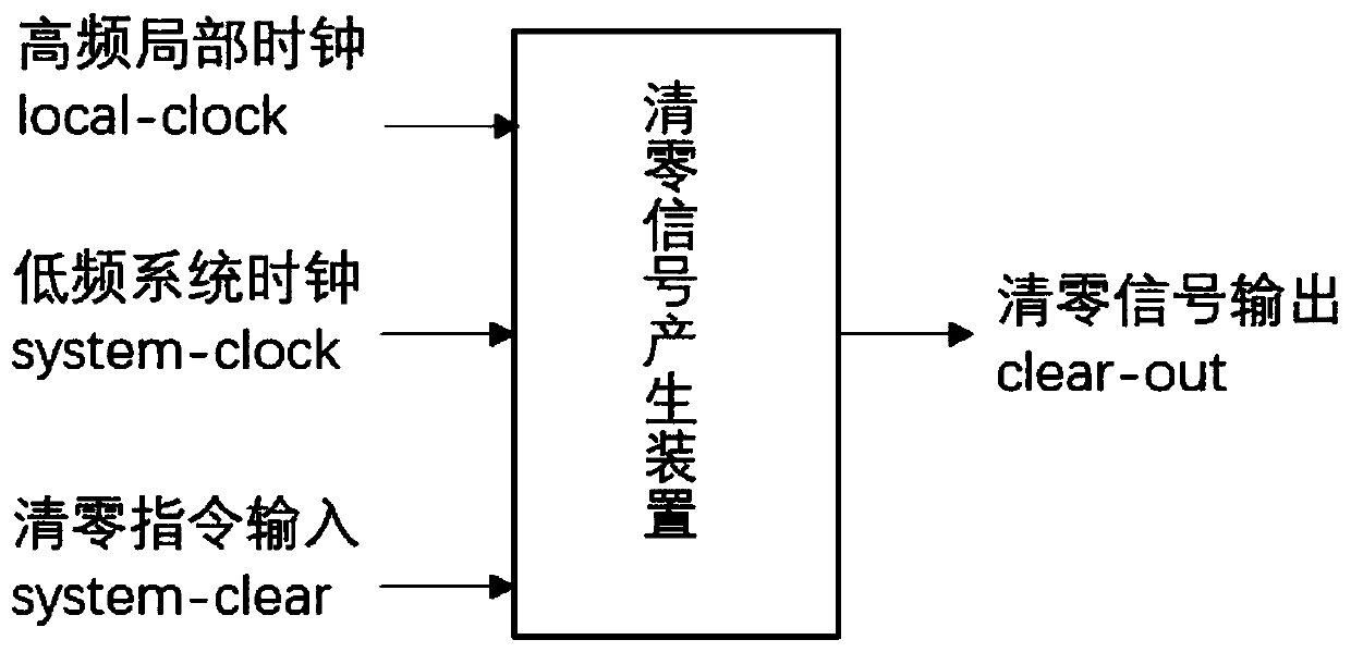
[0026] In the process of designing a pipeline-based superconducting processor, the inventor needs to provide a clearing signal that meets the timing requirements for the superconducting circuit register. There is no specific and practical clearing signal generating device in the prior art. Therefore, the present invention is used in superconducting circuit design. After obtaining a clearing command signal, it provides a specific clearing signal generating device and method for superconducting registers that meet the actual working sequence requirements of superconducting circuits.

[0027] The present invention includes following key points:

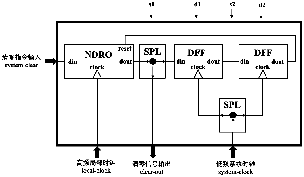
[0028] Key point 1, the clearing signal generating device includes a clearing command signal input port, a high-frequency local clock input port, a low-frequency system clock input port, and a clearing signal output port;

[0029] Key point 2, after receiving a clearing instruction signal, the clearing signal generating device starts to...


PUM


Abstract

The invention provides a zero clearing method and system for a superconducting circuit. The method comprises the following steps: sending a zero clearing instruction signal to an instruction input interface of a non-destructive read-out register, wherein the non-destructive reading register outputs data to a first magnetic flux quantum separation device according to the high-frequency local clocksignal, and the first magnetic flux quantum separation device separates the output data into a zero clearing signal and a trigger signal and inputs the zero clearing signal to a superconducting register between pipeline stages of the superconducting processor; inputting a low-frequency system clock signal to a second magnetic flux quantum separation device, wherein the second magnetic flux quantumseparation device splits the low-frequency system clock signal into a first low-frequency system clock pulse and a second low-frequency system clock pulse; the first D trigger outputs a signal pulseaccording to a trigger signal and a first low-frequency system clock pulse, the second magnetic flux quantum separation device outputs a delay pulse according to the signal pulse and a second low-frequency system clock pulse, and the non-destructive reading register resets according to the delay pulse so as to stop outputting a zero clearing signal.

Description

technical field [0001] The invention relates to the design field of superconducting circuit components in superconducting computers, and in particular to a method and system for clearing superconducting circuits. Background technique [0002] Superconducting circuit technology is an important technology development direction of computers in the future. Countries such as the United States, Japan, the United Kingdom, and South Africa all attach importance to the research and development of superconducting devices. There are also many domestic units that continue to carry out research and development of superconducting components and computers. Work. The design of existing superconducting circuit components is mostly based on traveling wave and flowing water, without the traditional flip-flop concept, which makes it difficult to realize the register function. In the world, research and development institutions such as the United States and Japan have proposed to use limited un...

Claims


Application Information

Patent Timeline
IPC IPC(8): H03K3/012H03K5/14H03K3/86
CPCH03K3/012H03K3/86H03K5/14
Inventor 张志敏唐光明张阔中轩伟瞿佩瑶杨佳洪
Owner INST OF COMPUTING TECH CHINESE ACAD OF SCI
Learn More