Shielded gate field effect transistor and method of forming the same

A field-effect transistor and shielding gate technology, which is applied in semiconductor devices, semiconductor/solid-state device manufacturing, electrical components, etc., can solve problems such as short-circuiting of the middle gate electrode and shielding electrode, so as to reduce the difficulty of filling and ensure isolation Performance, the effect of improving filling performance

Active Publication Date: 2022-08-02
SEMICON MFG ELECTRONICS (SHAOXING) CORP
View PDF5 Cites 0 Cited by
  • Summary
  • Abstract
  • Description
  • Claims
  • Application Information

AI Technical Summary

Problems solved by technology

[0004] The purpose of the present invention is to provide a method for forming a shielded gate field effect transistor to solve the problem of easy short circuit between the gate electrode and the shielding electrode in the existing shielded gate field effect transistor

Method used


Image

  • Shielded gate field effect transistor and method of forming the same
  • Shielded gate field effect transistor and method of forming the same
  • Shielded gate field effect transistor and method of forming the same

Examples


Embodiment Construction

[0068] As described in the background art, when the isolation layer between the gate electrode and the shield electrode is currently prepared, it is easy to cause a gap in the formed isolation layer. In view of this technical problem, the inventors of the present invention have found after research that the reason why gaps are easily formed in the isolation layer between the gate electrode and the shield electrode is that the insulating filling material used to form the isolation layer has voids, Furthermore, when the insulating filling material is etched to form the isolation layer, a gap will be generated in the formed isolation layer.

[0069] Specifically, a method for forming a shielded gate field effect transistor generally includes the following steps.

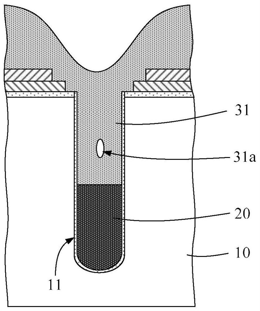
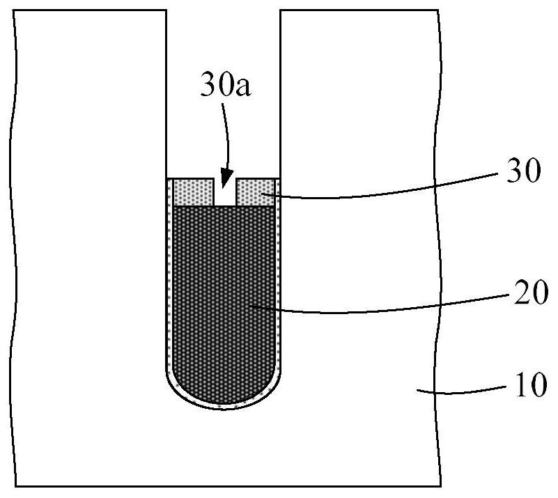
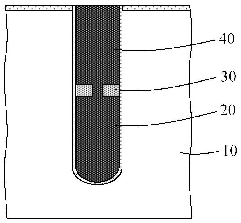
[0070] The first step, specific reference Figure 1a As shown, a substrate 10 is provided, and a gate trench 11 is formed in the substrate 10 , and a shield electrode 20 is formed at the bottom of the gate trench 11 . ...


PUM

PropertyMeasurementUnit
sizeaaaaaaaaaa
sizeaaaaaaaaaa
thicknessaaaaaaaaaa

Abstract

The present invention provides a shielded gate field effect transistor and a method for forming the same. After the shielding electrode is formed, an isolation spacer with decreasing thickness from bottom to top is formed on the sidewall of the gate trench higher than the shielding electrode, so that the topography of the upper trench located above the shielding electrode is modified by the isolation spacer. In this way, the filling difficulty of the insulating filling layer can be reduced, and the filling performance of the insulating filling layer in the upper trench can be improved to avoid the occurrence of voids, and further, when the insulating filling layer is subsequently etched to form the isolation layer, a gap-free isolation layer can be formed to ensure the gate. Mutual isolation between electrode and shield electrode.

Description

technical field [0001] The present invention relates to the technical field of semiconductors, in particular to a shielded gate field effect transistor and a method for forming the same. Background technique [0002] Shielded gate field effect transistor (Shielded Gate Trench, SGT), because of its low gate-drain capacitance Cgd, low on-resistance, and high withstand voltage performance, which is more conducive to the flexible application of semiconductor integrated circuits. Specifically, in the shielded gate field effect transistor, by arranging the shielding electrode below the gate electrode, the gate-to-drain capacitance can be greatly reduced, and the drift region of the shielded gate field effect transistor also has higher impurity carriers concentration, which can provide additional benefits to the breakdown voltage of the device, and correspondingly lower on-resistance. [0003] Compared with other trench field effect transistors, although the shielded gate field ef...

Claims


Application Information

Patent Timeline
Patent Type & Authority Patents(China)
IPC IPC(8): H01L21/336H01L29/78
CPCH01L29/66477H01L29/78
Inventor 谢志平丛茂杰唐昊李枭
Owner SEMICON MFG ELECTRONICS (SHAOXING) CORP
Why Eureka
Try Eureka