A kind of electronic component diode pin processing method

A technology of electronic components and processing methods, which is applied in the manufacture of electrical components, semiconductor devices, semiconductor/solid-state devices, etc., can solve problems such as low work efficiency, diode extrusion damage, deviation, etc., to improve work efficiency and enhance work The effect of volume and deformation prevention

Active Publication Date: 2020-12-04
泰州港润投资发展有限公司
View PDF5 Cites 0 Cited by
  • Summary
  • Abstract
  • Description
  • Claims
  • Application Information

AI Technical Summary

Problems solved by technology

[0003] The following problems often exist in the bending operation of the existing electronic diode pins: a. When the existing diode pins are being bent, it is often necessary to directly bend the diode body with tweezers after the diode body is fixed. Greatly enhanced the workload of the workers, and the work efficiency is also relatively low, and it is easy to take place as the phenomenon that the diode is originally squeezed and damaged; b: the existing diode pins often use manual bending when performing bending operations The diode pins are bent in this way, the bending angle of the pins is not uniform, and there is a certain deviation, which affects the quality of the diode

Method used


Image

  • A kind of electronic component diode pin processing method
  • A kind of electronic component diode pin processing method
  • A kind of electronic component diode pin processing method

Examples


Embodiment Construction

[0035] The embodiments of the present invention will be described in detail below with reference to the accompanying drawings, but the present invention can be implemented in many different ways defined and covered by the claims.

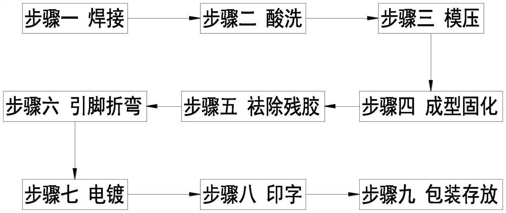
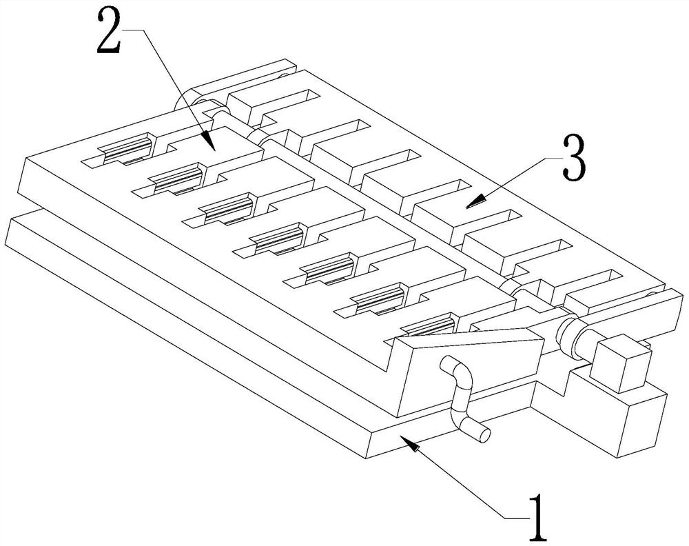
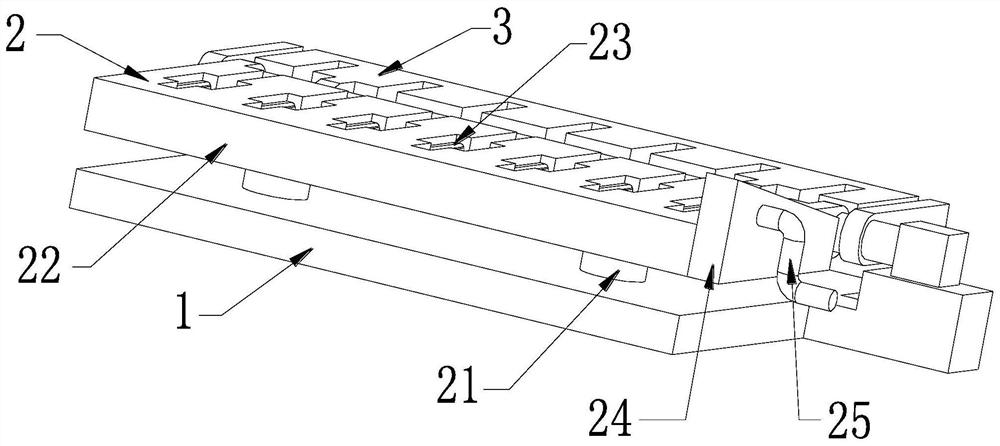
[0036] Such as Figure 1 to Figure 7 As shown, a method for processing diode pins of electronic components mainly includes the following steps:

[0037] Step 1, welding: use the solder piece to pass through a certain temperature to connect the chip to the metal pin;

[0038] Step 2, pickling: put the above-mentioned semi-finished product treated in step 1 into an acidic substance for washing, and chemically corrode the edge surface of the P-N junction of the chip to improve mechanical damage, remove impurities adsorbed on the surface, reduce the surface electric field, and make the P-N junction The breakdown of the junction first occurs from the body to obtain a reverse breakdown voltage close to the theoretical value and a very small surface leaka...


PUM


Abstract

The invention relates to an electronic component diode pin processing method. The method mainly comprises the following steps that: welding, acid pickling, mold pressing, forming and curing, residualglue removing, pin bending, electroplating, lettering, packaging and storing are carried out; and a used pin bending device comprises a mounting frame, a fixing plate and an overturning plate, a fixedplate is mounted on the mounting frame, and an overturning plate is arranged at the right end of the fixed plate in a rotary connection manner. The method can solve problems that when an existing steel plate is subjected to surface polishing operation: a, when diode pins are bent, a diode needs to be fixed, then tweezers are used for directly bending the diode pins, the workload is greatly increased, the working efficiency is low, and the phenomenon that a diode body is prone to being extruded and damaged is caused can be solved; and b, when the existing diode pins are bent, the diode pins are bent in a manual bending mode, so that the bending angles of the pins cannot be unified, a certain deviation exists, and the quality of the diode is influenced.

Description

technical field [0001] The invention relates to the technical field of diode processing, in particular to a method for processing diode pins of electronic components. Background technique [0002] Diode is an electronic component with two electrodes, and the diode only allows current to flow in one direction, so it is widely used in electronic products. Now electronic diodes need to be welded, pickled, and molded for a long time during production. , Forming and curing, removing residual glue, pin bending, electroplating, printing, packaging and storage, etc., among which pin bending is more directly related to the use of diodes. [0003] The following problems often exist in the bending operation of the existing electronic diode pins: a. When the existing diode pins are being bent, it is often necessary to directly bend the diode body with tweezers after the diode body is fixed. Greatly enhanced the workload of the workers, and the work efficiency is also relatively low, an...

Claims


Application Information

Patent Timeline
Patent Type & Authority Patents(China)
IPC IPC(8): H01L21/48H01L29/861B21F1/00
CPCB21F1/004H01L21/4814H01L21/4885H01L21/4896H01L29/861
Inventor 林瑞
Owner 泰州港润投资发展有限公司
Why Eureka
Try Eureka