

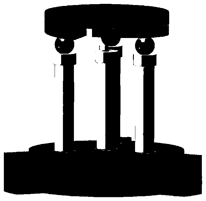
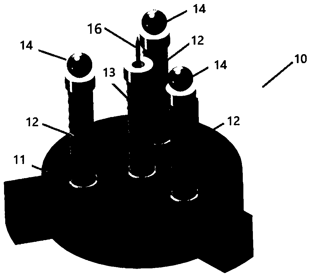
Scanning tunneling microscope and sample holder thereof
A technology for scanning tunnels and sample holders, which is applied in the field of nanoscale characterization, and can solve problems such as the inability to integrate multiple electrodes
- Summary
- Abstract
- Description
- Claims
- Application Information
AI Technical Summary
Problems solved by technology
Method used
Image

Examples
Embodiment 1
[0064] Embodiment 1: Common STM function.
[0065] Such as Figure 5 As shown, one of the electrodes on the sample holder is connected to the bias voltage, and the probe lead is connected to the STM preamplifier. STM can be used to characterize the surface atomic resolution morphology, electronic state and single atom or functions such as single molecule manipulation.
Embodiment 2
[0066] Example 2: Apply gate voltage to regulate the electronic state of the few-layer 2D material, and use STM to characterize it.
[0067] Such as Figure 6 As shown, terminal 1 is connected to the few-layer 2D material, and Bias voltage is applied; terminal 4 is connected to the probe, and the tunneling current is measured. It can complete basic STM functions. Terminal 2 is connected to the gate, and the gate voltage is added to regulate the electronic state. It can be used to characterize the variation of electronic states of few-layer 2D materials with gate voltage.
Embodiment 3
[0068] Example 3: STM combined with transport measurements.
[0069] Such as Figure 7 As shown, in the STM mode, the Bias voltage is applied to the 2-terminal, and the tunneling current is measured at the 4-terminal. In the transport mode of measurement, the 1 terminal and 2 terminal are respectively connected to the two ends of the material to be tested, and the voltage is applied to both ends to measure the current; the 3 terminal and 4 terminal can measure the voltage. By changing the position of the probe, the conductance information at different positions can be measured.
PUM
 Abstract
Description
Claims
Application Information