Transfer substrate, driving backboard, transfer method and display device

A technology for transferring substrates and driving backplanes, used in identification devices, static indicators, instruments, etc., can solve the problems of low transfer yield of miniature light-emitting diodes, improve the transfer yield, not easy to lose and wear, and improve the accuracy of the transfer. The effect of bit precision

Active Publication Date: 2020-06-05
FUZHOU BOE OPTOELECTRONICS TECH CO LTD +1
View PDF5 Cites 2 Cited by
  • Summary
  • Abstract
  • Description
  • Claims
  • Application Information

AI Technical Summary

Problems solved by technology

[0004] The embodiment of the present invention provides a transfer substrate, a driving backplane, a transfer method and a display device, which are used to solve the transfer of micro light emitting diodes existing in the prior art The problem of low yield

Method used


Image

  • Transfer substrate, driving backboard, transfer method and display device
  • Transfer substrate, driving backboard, transfer method and display device
  • Transfer substrate, driving backboard, transfer method and display device

Examples


Embodiment Construction

[0050] To solve the problem of low transfer yield of micro light emitting diodes in the prior art, embodiments of the present invention provide a transfer substrate, a driving backplane, a transfer method and a display device.

[0051] The specific implementation manners of the transfer substrate, the driving backplane, the transfer method and the display device provided by the embodiments of the present invention will be described in detail below with reference to the accompanying drawings. The thickness and shape of each film layer in the drawings do not reflect the real scale, and the purpose is only to illustrate the content of the present invention.

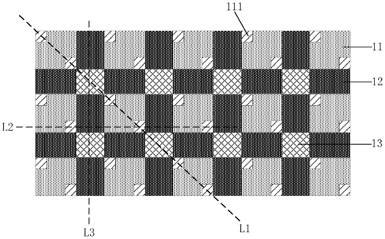
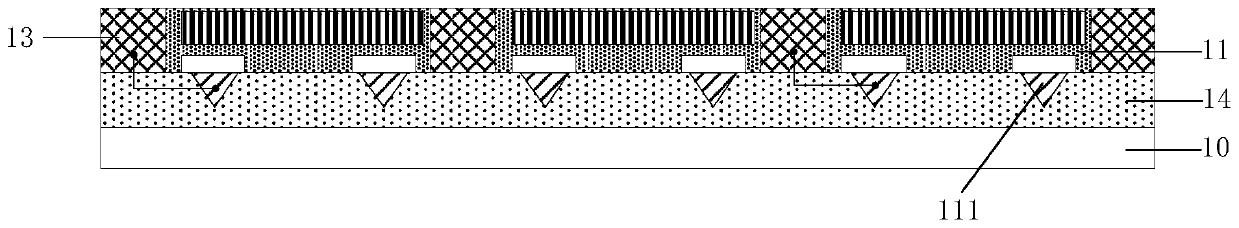
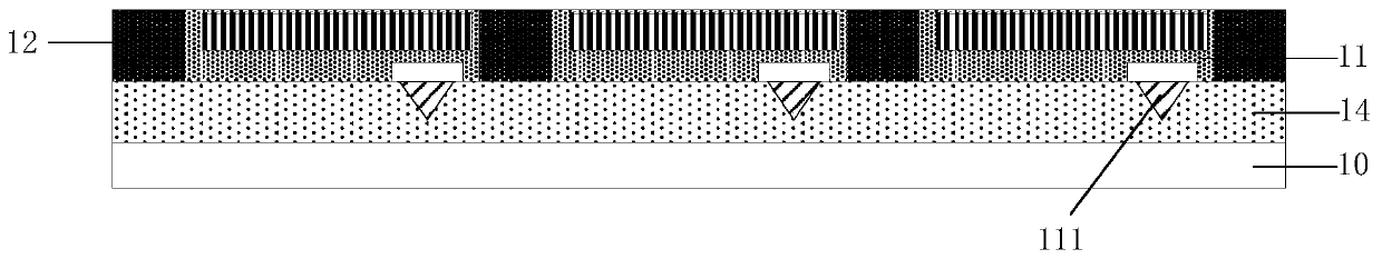
[0052] In a first aspect, an embodiment of the present invention provides a transfer substrate, figure 1 It is a schematic diagram of the planar structure of the transfer substrate provided by the embodiment of the present invention, figure 2 for figure 1 The cross-sectional schematic diagram at the dotted line L1 in the ...


PUM

PropertyMeasurementUnit
sizeaaaaaaaaaa

Abstract

The invention discloses a transfer substrate, a driving backboard, a transfer method and a display device, and the transfer substrate comprises a base material, a plurality of light emitting diodes located on the base material, and a plurality of connection structures located between the adjacent light emitting diodes. The connecting structures are used for connecting the adjacent light emitting diodes, the plurality of connecting structures respectively correspond to the alignment structures on the driving back plate, and the plurality of connecting structures are used for aligning with the corresponding alignment structures in the transferring process of the light emitting diode. According to the transfer substrate Provided by the embodiment of the invention, the plurality of light emitting diodes can be connected into a whole through a plurality of connecting structures; in the transferring process of the light-emitting diodes, the light-emitting diodes are not prone to being lost and abraded; and, in the transferring process of the light-emitting diodes, alignment can be conducted through the multiple connecting structures and the corresponding connecting structures, the light-emitting diodes are aligned with the corresponding driving electrode set, the alignment precision is improved, dislocation is reduced, and the transferring yield of the light-emitting diodes is increased.

Description

technical field [0001] The invention relates to the field of display technology, in particular to a transfer substrate, a driving backplane, a transfer method and a display device. Background technique [0002] Due to the advantages of self-illumination, simple structure, small size and energy saving of micro light emitting diode (Micro LED), micro light emitting diode display technology will become the next generation of revolutionary technology. Specifically, the power consumption of Micro LED display is only 10% of a liquid crystal display (Liquid Crystal Display, LCD) is 50% of an organic light-emitting diode display (Organic Light-Emitting Diode, OLED). In addition, compared with OLED displays, which are also self-luminous displays, under the same power, the screen brightness of Micro LED displays is three times higher than that of OLED displays, the display color gamut is as high as 120%, and it has better material stability. sex and no image sticking. [0003] Due t...

Claims


Application Information

Patent Timeline
Patent Type & Authority Applications(China)
IPC IPC(8): H01L21/683H01L21/67H01L27/15G06F3/044G09F9/33G09G3/32
CPCH01L21/6835H01L21/67144H01L27/156G09F9/33G09G3/32G06F3/044
Inventor 余仁惠谢洪洲胡晔郑上涛查文陈美珍陈信李增荣侯清娜刁凯
Owner FUZHOU BOE OPTOELECTRONICS TECH CO LTD
Why Eureka
Try Eureka