Image sensor and image processing method

An image sensor and pixel technology, applied in the field of image processing, can solve the problems of high power consumption, large pixel size, and large thickness of CMOS image sensors

Inactive Publication Date: 2020-06-05
GUANGDONG OPPO MOBILE TELECOMM CORP LTD
View PDF9 Cites 0 Cited by
  • Summary
  • Abstract
  • Description
  • Claims
  • Application Information

AI Technical Summary

Problems solved by technology

[0003] Generally, the pixel array commonly used in CMOS image sensors is mainly composed of square pixel units, in which photodiode (Photo Diode, PD) structures are arranged for light absorption and photoelectric conversion; CMOS image sensors use square pixel units in a quadrangular array. Arrangement in the same way, using the pixel unit in the positive direction to absorb the corresponding RGB monochromatic light, at this time, the arrangement

Method used


Image

  • Image sensor and image processing method
  • Image sensor and image processing method
  • Image sensor and image processing method

Examples


Example Embodiment

[0048] Example one

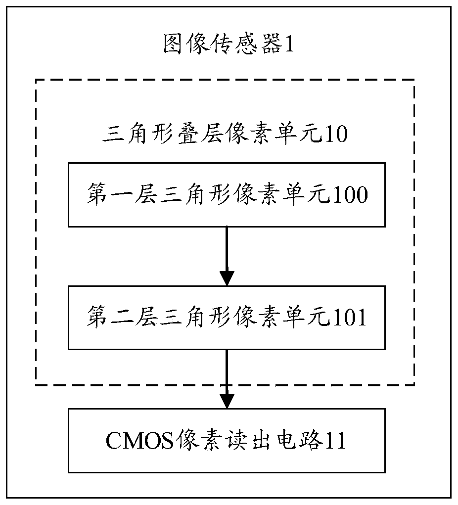
[0049] The embodiment of the present application provides an image sensor 1, such as figure 1 As shown, the image sensor 1 includes:

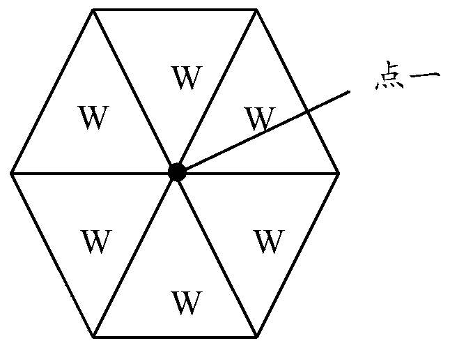
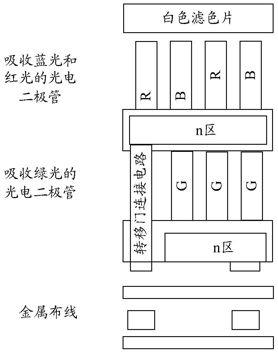
[0050] A triangular stacked pixel unit 10 composed of a first layer of triangular pixel units 100 and a second layer of triangular pixel units 101, wherein the first layer of triangular pixel units 100 includes two sizes of photodiode PD columns, and the second layer The layered triangular pixel unit 101 includes PD columns of one size in addition to the two sizes; the triangular stacked pixel unit 10 is used to absorb the RGB three-color light by using the three-size PD columns, and combine the RGB three-color light The corresponding optical signal is converted into an electrical signal

[0051] The CMOS pixel readout circuit 11 connected to the output terminal of the triangular stacked pixel unit 10 is used to amplify the electrical signal and read out the electrical signal.

[0052] The image sensor proposed in the embodiment o...

Example Embodiment

[0098] Example two

[0099] The embodiment of the application provides an image processing method, which is applied to an image sensor. The image sensor includes a triangular stacked pixel unit composed of a first layer of triangular pixel units and a second layer of triangular pixel units and a CMOS pixel readout circuit. The triangular pixel unit includes PD columns of two sizes, and the second layer of triangular pixel unit includes PD columns of one size in addition to the two sizes, such as Image 6 As shown, the method includes:

[0100] S101. The PD columns of the two sizes of the triangular pixel unit of the first layer are used to absorb two RGB monochromatic lights respectively, and the optical signals corresponding to the two RGB monochromatic lights are converted into electrical signals corresponding to the two RGB monochromatic lights.

[0101] The image processing method provided by the embodiment of the present application is suitable for performing image processing o...

Example Embodiment

[0115] Example three

[0116] The embodiment of the present application provides a storage medium on which a computer program is stored. The computer-readable storage medium stores one or more programs. The one or more programs can be executed by one or more processors and are applied to images. In the sensor 1, the image sensor includes a triangular stacked pixel unit composed of a first layer of triangular pixel units and a second layer of triangular pixel units, and a CMOS pixel readout circuit. The first layer of triangular pixel units includes two sizes of PD column, the second layer of triangular pixel units includes PD columns of one size except two sizes, and the computer program implements the image processing method described in the second embodiment.

[0117] Specifically, when a program instruction corresponding to an image processing method in this embodiment is read or executed by an electronic device, it includes the following steps:

[0118] The two-size PD columns o...


PUM

PropertyMeasurementUnit
Diameteraaaaaaaaaa
Diameteraaaaaaaaaa
Diameteraaaaaaaaaa

Abstract

The embodiment of the invention provides an image sensor and an image processing method. The image sensor comprises a triangular laminated pixel unit composed of a first layer of triangular pixel unitand a second layer of triangular pixel unit, wherein the first layer of triangular pixel unit comprises photodiode PD columns of two sizes, the second layer of triangular pixel unit comprises PD columns of one size except the two sizes, a triangular laminated pixel units are used for absorbing RGB three-color light by utilizing PD columns of three sizes and converting optical signals corresponding to the RGB three-color light into electric signals; and a CMOS pixel reading circuit which is connected with the output end of the triangular laminated pixel unit and is used for amplifying the electric signal and reading the electric signal.

Description

technical field [0001] The present application relates to the field of image processing, in particular to an image sensor and an image processing method. Background technique [0002] Complementary Metal-Oxide Semiconductor (CMOS, Complementary Metal-Oxide Semiconductor) image sensor (Complementary Metal-Oxide Semiconductor Image Sensor, CMOS Image Sensor) has the characteristics of high integration, low power consumption, fast speed and low cost. Pixel products are widely used. [0003] Generally, the pixel array commonly used in CMOS image sensors is mainly composed of square pixel units, in which photodiode (Photo Diode, PD) structures are arranged for light absorption and photoelectric conversion; CMOS image sensors use square pixel units in a quadrangular array. Arrangement in the same way, using the pixel unit in the positive direction to absorb the corresponding RGB monochromatic light, at this time, the arrangement density of the square pixel unit is low, which lead...

Claims


Application Information

Patent Timeline
IPC IPC(8): H04N5/374H04N5/378H04N5/369H01L27/146
CPCH01L27/14609H01L27/14645H04N25/76H04N25/79H04N25/75
Inventor 杨鑫
Owner GUANGDONG OPPO MOBILE TELECOMM CORP LTD
Why Eureka
Try Eureka