Organic light-emitting display panel, manufacturing method thereof and display device

A light-emitting display and organic technology, which is applied in semiconductor/solid-state device manufacturing, semiconductor devices, electrical components, etc., can solve the problems of uneven edge effect area of ​​OLED substrate, poor uniformity of film formation of light-emitting layer, etc., achieve simple solvent atmosphere, improve The uniformity of film formation and the effect of improving printing efficiency

Active Publication Date: 2020-06-12
HEFEI BOE ZHUOYIN TECH CO LTD +1
View PDF11 Cites 0 Cited by
  • Summary
  • Abstract
  • Description
  • Claims
  • Application Information

AI Technical Summary

Problems solved by technology

[0005] The inventors found that organic light-emitting display substrates (OLED substrates) made by inkjet printing, especially large-size OLED substrates, generally have the problem of poor film-forming uniformity of the light-emitting layer.
Therefore, during the printing process of the ent

Method used


Image

  • Organic light-emitting display panel, manufacturing method thereof and display device
  • Organic light-emitting display panel, manufacturing method thereof and display device
  • Organic light-emitting display panel, manufacturing method thereof and display device

Examples


Embodiment Construction

[0029] Embodiments of the present invention are described in detail below, examples of which are shown in the drawings, wherein the same or similar reference numerals designate the same or similar elements or elements having the same or similar functions throughout. The embodiments described below by referring to the figures are exemplary only for explaining the present invention and should not be construed as limiting the present invention.

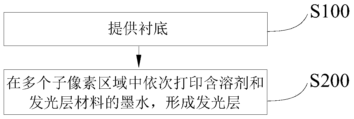
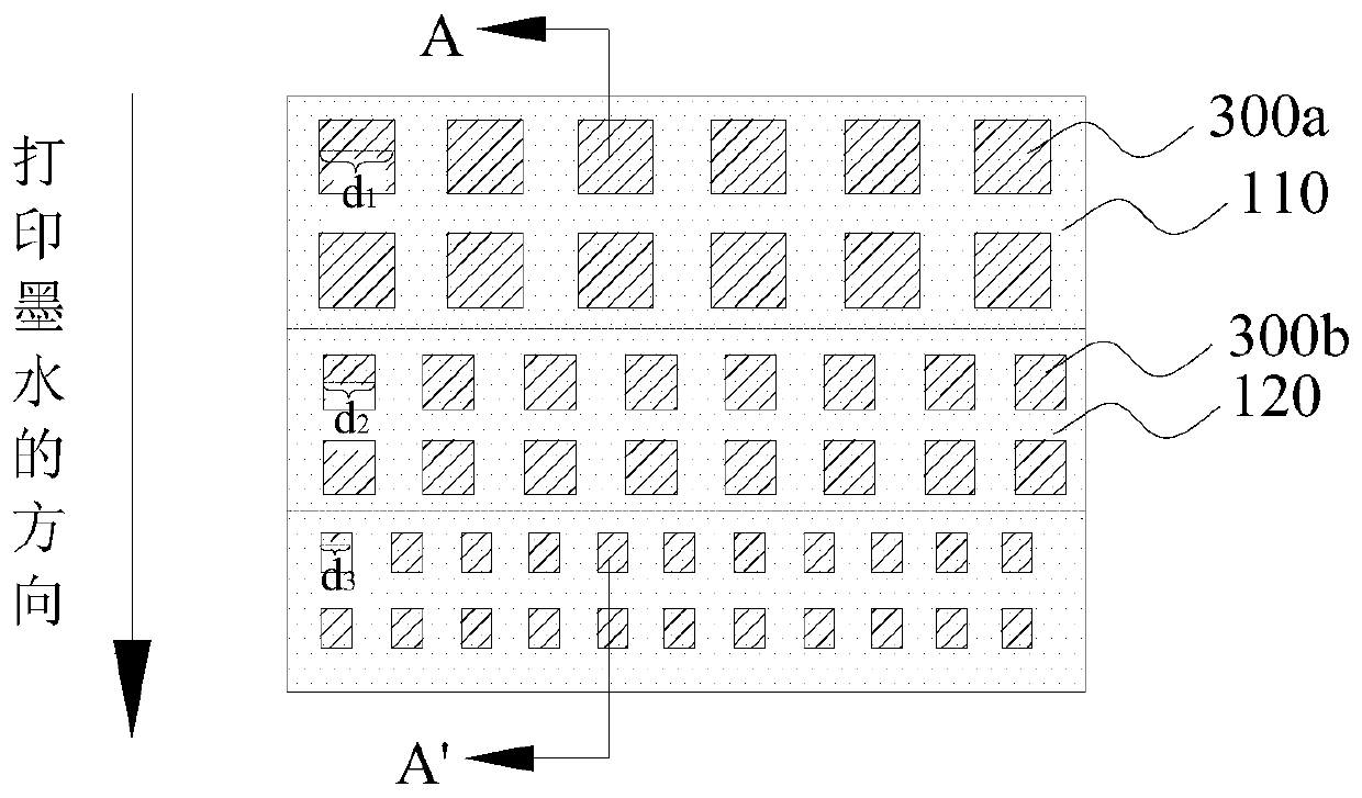
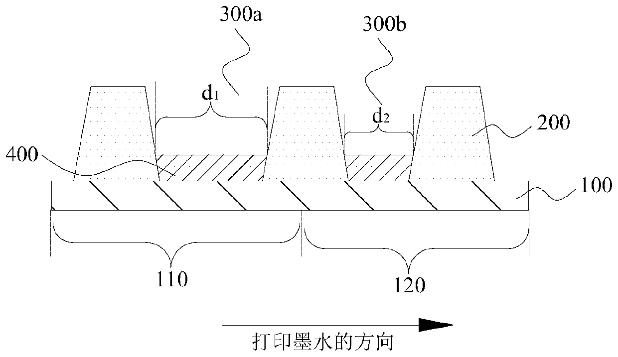
[0030]In one aspect of the invention, the invention provides a method for manufacturing an organic light emitting display panel. In this method, by making the opening ratios at different positions on the substrate different, or making the concentration of the solvent in the ink printed at different positions different, the amount of solvent in the sub-pixel area printed first can be more, and the sub-pixel area printed later can have a larger amount of solvent. The amount of solvent in the solvent is less, so it can better avoid the prob...


PUM


Abstract

The invention discloses an organic light-emitting display panel, a manufacturing method thereof and a display device. The invention provides the manufacturing method for the organic light-emitting display panel, and the method comprises the steps: providing a substrate which is provided with a pixel defining layer, and enabling the pixel defining layer to define a plurality of sub-pixel regions; sequentially printing ink containing a solvent and a light-emitting layer material in the plurality of sub-pixel regions to facilitate formation of a light-emitting layer, wherein the direction of theprinting ink and the concentration of the solvent in the ink meet at least one of the following conditions: the aperture ratios at different positions on the substrate are different, and the directionof the printing ink is the direction extending from the position with the larger aperture ratio of the sub-pixel area to the position with the smaller aperture ratio of the sub-pixel area; the concentrations of the solvents in the ink printed at different positions on the substrate are different, and the concentrations of the solvents are reduced in the direction of the printing ink. Therefore, the method can improve the film forming uniformity of the light-emitting layer, facilitates the design of a narrow frame, and improves the display quality of an OLED and the quality of a product.

Description

technical field [0001] The present invention relates to the field of display technology, in particular, to an organic light emitting display panel, a manufacturing method thereof, and a display device. Background technique [0002] Organic electroluminescence (OLED) display technology is characterized by self-illumination, wide viewing angle, high contrast ratio, low power consumption, extremely high response speed, ultra-thin weight, flexible display, rollable screen, strong temperature adaptability, and simple manufacturing process, etc. Advantages, has become a research hotspot in the field of optoelectronic display technology. The inkjet printing method has the advantages of simple operation, low cost, simple process, and easy realization of large size, and is widely used in the production of organic light-emitting display panels. Specifically, the materials used to make OLED display substrates can be dissolved in specific inkjet printing solvents to form inkjet printin...

Claims


Application Information

Patent Timeline
IPC IPC(8): H01L51/56H01L27/32
CPCH10K59/00H10K71/135H10K71/00
Inventor 贾文斌叶志杰
Owner HEFEI BOE ZHUOYIN TECH CO LTD
Why Eureka
Try Eureka