Ultra-thin wave absorber based on deep sub-wavelength slits

A deep subwavelength, wave absorber technology, applied in the field of ultra-thin wave absorbers, can solve the problem of poor wave absorption effect, and achieve the effect of light weight, simple structure and cost reduction

Inactive Publication Date: 2020-06-16
ZHEJIANG UNIV
View PDF3 Cites 4 Cited by
  • Summary
  • Abstract
  • Description
  • Claims
  • Application Information

AI Technical Summary

Problems solved by technology

If the thickness of the structure is further reduced, the absorbing effect will become worse

Method used


Image

  • Ultra-thin wave absorber based on deep sub-wavelength slits
  • Ultra-thin wave absorber based on deep sub-wavelength slits
  • Ultra-thin wave absorber based on deep sub-wavelength slits

Examples


Embodiment 1

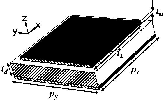
[0021] Set the working frequency to 2.21 GHz and the working wavelength to 135.7 mm. Low-loss doped PTFE plate is selected as the dielectric material, ε = 3.6, tan δ = 0.004. The metal material is copper, and the thickness is a typical value of 18 μm under the copper clad process. .

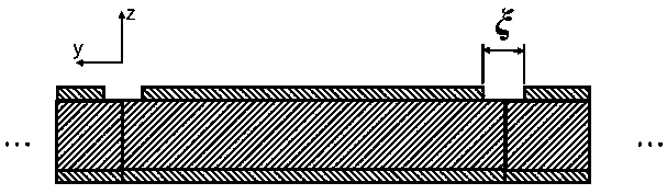
[0022] The side length of the metal patch is set to l ≈ lambda / 2 / √ ε = 34.3 mm, the thickness of the dielectric spacer is set to t d = lambda / 300 = 0.45 mm, and the width of the air slit between the patches was set to 0.5 mm. Scanning with CST t d and l , and after fine-tuning twice, the final scale parameter is obtained, t d = 0.25 mm, l = 35 mm.

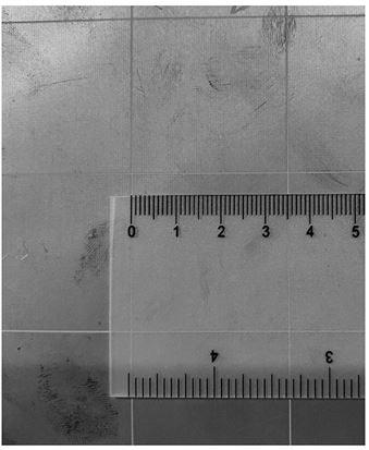
[0023] Both material production and structural processing can rely on mature board manufacturers and circuit board processors. Produced absorbers such as image 3 with 4 As shown, the width and thickness are in line with the design values. The simulated absorbing effect (magnitude of reflection coefficient) of this abso...


PUM


Abstract

The invention discloses an ultra-thin wave absorber based on deep sub-wavelength slits, which is characterized in that the thickness of a unit structure of the ultra-thin wave absorber is a deep sub-wavelength scale, namely, one percent wavelength magnitude and below, the ultra-thin wave absorber is divided into three layers along the height direction, namely, a metal patch, a dielectric spacer layer and a metal back plate from top to bottom, and an air slit with a deep sub-wavelength width is arranged between adjacent metal patches; the dielectric spacer layer is made of a low-loss material with the loss tangent value tan[delta] being less than 0.01, or the dielectric spacer layer is made of a lossless material; the wave absorbing wavelength is changed by changing the size of the metal patch and adjusting the thickness of the dielectric spacer layer so as to achieve wave absorption, and the wave absorber can work in all frequency bands from terahertz, microwaves to radio frequency. The thickness of the wave absorber is very small, the thickness of the wave-absorbing device is reduced to a few hundredths of wavelength from the traditional a few tenths of wavelength, and the wave absorber is very thin and light in weight and has certain flexibility; a mature circuit board process can be adopted for manufacturing, and the cost is reduced; and the wave absorbing effect is not sensitive to the incident angle, and the wave absorber has a conformal advantage and can cover the curved surface.

Description

technical field [0001] The invention belongs to the field of electromagnetic fields and electromagnetic waves, in particular to an ultra-thin absorber based on deep subwavelength slits. Background technique [0002] Microwave absorbers have extensive and important applications in the fields of stealth, detection, and sensing. In many application scenarios, it is desired to reduce the thickness of the absorbing structure, thereby reducing the thickness and weight of the device, or improving the sensitivity and response speed of the device. When using natural materials for electromagnetic absorption, the materials need to have high material loss, and the thickness of the structure is usually about a quarter of the wavelength; when it is required to further reduce the thickness of the structure, special materials such as ferromagnetism need to be used. This undoubtedly increases the cost of preparation, and this approach cannot be extended to terahertz and other wave bands, be...

Claims


Application Information

Patent Timeline
Patent Type & Authority Applications(China)
IPC IPC(8): H01Q17/00G02B1/00G02B5/00
CPCG02B1/002G02B5/003H01Q17/00
Inventor 何赛灵金毅付济超
Owner ZHEJIANG UNIV
Why Eureka
Try Eureka