A High Side Conductance Enhanced Power Switch Driving Circuit

A driving circuit and power switch technology, which is applied in electronic switches, output power conversion devices, electrical components, etc., can solve problems such as low hole mobility, large conduction resistance, and occupied output resistance, and achieve a simplified design method , Improving the current drive capability and reducing the on-resistance value

Active Publication Date: 2021-12-03
成都市硅海武林科技有限公司
View PDF5 Cites 0 Cited by
  • Summary
  • Abstract
  • Description
  • Claims
  • Application Information

AI Technical Summary

Problems solved by technology

Because the power devices used are limited by the existing process conditions, chip area and manufacturing cost, it is difficult to integrate N-type power devices and P-type power devices in the same chip and the same substrate.
[0004] In the existing switch driving circuit based on a single N-type device, since the source voltage of the N-type device is floating, when it is fully turned on, the source voltage will be close to the power supply voltage due to its low on-resistance characteristics; When the device is off, its source voltage is pulled down to ground, so in order to reduce the loss when the device is turned on, the drive circuit needs an additional boost circuit, such as a charge pump circuit or a bootstrap circuit, to generate a voltage higher than the chip supply voltage Voltage to complete the control of the switch, and an additional boost circuit will increase the cost and complexity of the circuit
[0005] However, for a switch drive circuit based on a single P-type device, due to the low mobility of holes, the on-resistance value per unit area is relatively large, so a device that occupies a larger chip area is required to reduce the output resistance; in the case of heavy load In this case, the loss on the P-type power device is serious, and it will cause the device to heat up or even burn out.

Method used


Image

  • A High Side Conductance Enhanced Power Switch Driving Circuit
  • A High Side Conductance Enhanced Power Switch Driving Circuit
  • A High Side Conductance Enhanced Power Switch Driving Circuit

Examples


Embodiment Construction

[0031] The technical solution of the present invention will be described in detail below in conjunction with the accompanying drawings and specific embodiments.

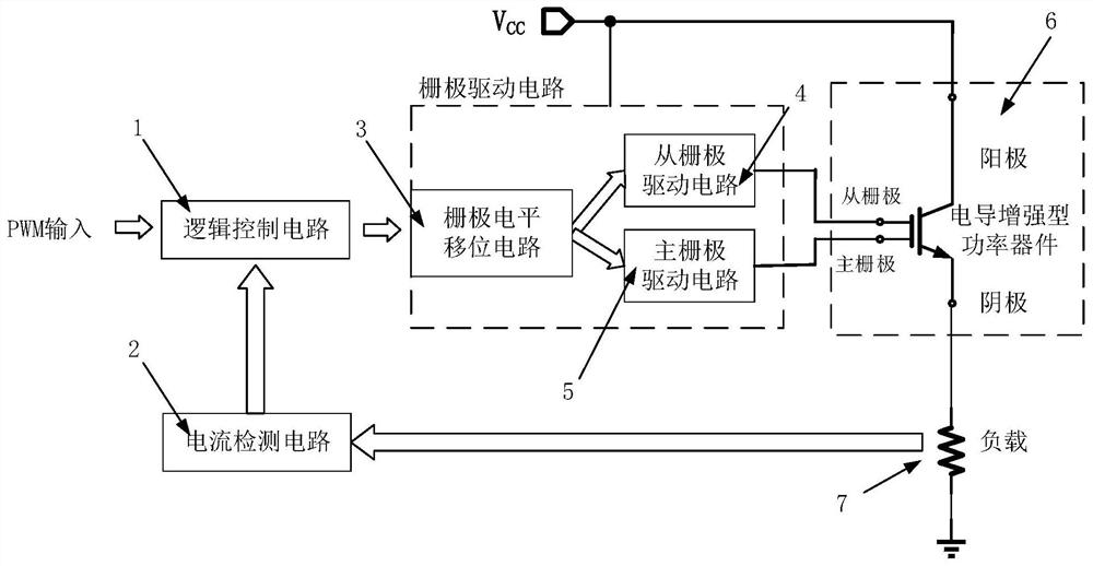
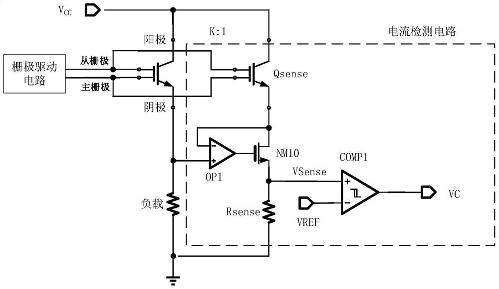
[0032] Such as figure 1 As shown, a high-side conductance-enhanced power device drive circuit includes: a conductance-enhanced power device 6, a current detection circuit 2, a logic control circuit 1, a gate level shift circuit 3, a main gate drive circuit 5, a slave Gate drive drive circuit 4, load 7 and power supply V CC .

[0033] The conductance-enhanced power device 6 has a main gate, a slave gate, an anode and a cathode, the conductance-enhanced power device main gate is connected to the output end of the main gate drive circuit, the slave gate is connected to the output end of the slave gate drive circuit, and the anode is connected to Power V CC , the cathode is grounded through the load; the conductance-enhanced power device is placed on the high side, and different operating modes are switched according ...


PUM


Abstract

The invention discloses a high-side conductance enhanced power switch drive circuit, which belongs to the technical field of electronic circuits. The present invention uses a gate level shift circuit to convert a gate level shift control signal output by a logic circuit into a set of signals with opposite phases, and then passes through a gate drive structure composed of a master gate drive and a slave gate drive circuit. , to drive a conductance-enhanced power device. Using this gate drive method not only realizes the performance of the traditional single power switch drive circuit, but also makes full use of all the conductive carriers in the semiconductor, which solves the problem of insufficient drive capability of a single P-type power switch and single N-type power switch. The complexity of the switch drive circuit can effectively reduce the on-resistance value, improve the current drive capability, and simplify the design method under the same chip area.

Description

technical field [0001] The invention belongs to the technical field of electronic circuits, and in particular relates to a high-side conductance enhanced power switch driving circuit. Background technique [0002] The high-side power switch drive circuit is a kind of integrated power device, gate drive circuit and protection circuit in the same chip. It has the characteristics of small size, light weight, high power density and high reliability. are widely used in. The high-side gate drive circuit is a non-important circuit. Its function is to drive and control the on and off of the high-side power device, and maintain this state until the arrival of the next control signal. The gate drive circuit determines the Can make full use of power device performance. [0003] Traditional switching drive circuits based on high-side power devices usually use a single N-type power device or P-type power device as a high-side switch tube. Because the power devices used are limited by ...

Claims


Application Information

Patent Timeline
Patent Type & Authority Patents(China)
IPC IPC(8): H02M1/08H03K17/94
CPCH02M1/08H03K17/94
Inventor 李俊宏刘健汤宇
Owner 成都市硅海武林科技有限公司
Why Eureka
Try Eureka