
Resistive random access memory unit and preparation method

A technology of resistive variable memory and resistive variable unit, which is applied in the field of memory and can solve problems such as unfavorable high-density integration and increased unit area

Active Publication Date: 2020-06-19
SHANGHAI INTEGRATED CIRCUIT RES & DEV CENT
View PDF7 Cites 8 Cited by
  • Summary
  • Abstract
  • Description
  • Claims
  • Application Information

AI Technical Summary

Problems solved by technology

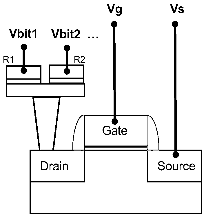
However, limited by the process rules such as line width and spacing, the conventional 1TnR structure usually increases the cell area significantly, which is not conducive to high-density integration

Method used


Image

  • Resistive random access memory unit and preparation method
  • Resistive random access memory unit and preparation method
  • Resistive random access memory unit and preparation method

Examples


Embodiment Construction

[0042] The specific embodiment of the present invention will be further described in detail below in conjunction with the accompanying drawings.

[0043] It should be noted that, in the following specific embodiments, when describing the embodiments of the present invention in detail, in order to clearly show the structure of the present invention for the convenience of description, the structures in the drawings are not drawn according to the general scale, and are drawn Partial magnification, deformation and simplification are included, therefore, it should be avoided to be interpreted as a limitation of the present invention.

[0044]In the following specific embodiments of the present invention, please refer to Figure 5 , Figure 5 It is a structural schematic diagram of a 2TnR type resistive memory unit according to a preferred embodiment of the present invention. Such as Figure 5 As shown, the resistive memory cell structure proposed by the present invention is a re...


PUM


Abstract

The invention discloses a resistive random access memory unit. The resistive random access memory unit comprises two coupled transistors and n resistive random access units. The n resistive units areconnected in sequence through electrodes of the resistive units to form a horizontal laminate structure. Any two adjacent resistive random access units share the same electrode. Gates of the two transistors are used for respectively applying different control signals. The source electrodes of the two transistors are connected and used for jointly applying a source signal. The drain electrodes of the two transistors are connected with electrodes at one ends of m different resistive random access units in the n resistive random access units respectively, and electrodes at the other ends of the nresistive random access units are used for applying different bit signals respectively. The resistive random access memory in the 2TnR form is formed on the basis of the vertical channel transistor and the resistive random access units of the horizontal laminated structure. The binary and multi-valued storage functions can be simultaneously realized according to different operation time sequences. The unit area is controllable, and the resistive random access memory unit can be used for realizing a high-density resistive random access memory array and a high-density resistive random access memory chip.

Description

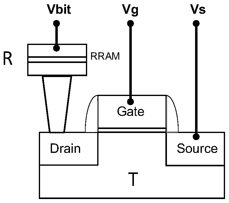
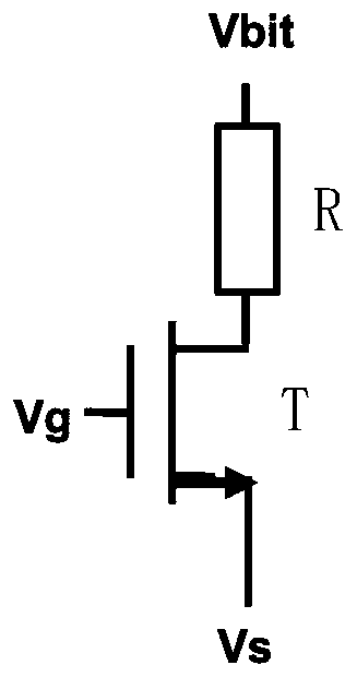
technical field [0001] The invention relates to the technical field of memory, in particular to a resistance variable memory unit capable of realizing binary or multi-value operation and a preparation method thereof. Background technique [0002] Resistive RAM (RRAM) is a new type of non-volatile memory. It has the advantages of high speed, low power consumption, non-volatility, high integration and compatibility with CMOS technology. It has become a new type of memory in recent years. One of the research hotspots, even commercial products have appeared. [0003] The cell structure of RRAM is the core of RRAM technology, and RRAM arrays and RRAM chips can only be constructed based on RRAM cells. [0004] The current mainstream RRAM cell structure is usually 1T1R structure, and its typical structure is as follows Figure 1-Figure 2 As shown, a transistor (T) and a resistive variable unit (R) are connected in series to form an RRAM unit. Its transistors usually use planar MO...

Claims


Application Information

Patent Timeline
Patent Type & Authority Applications(China)
IPC IPC(8): H01L27/24H01L45/00
CPCH10B63/34H10N70/253H10N70/8265H10N70/023H10N70/063H10N70/8833Y02D10/00H10N70/823H10N70/20
Inventor 郭奥
Owner SHANGHAI INTEGRATED CIRCUIT RES & DEV CENT
Learn More