Three-dimensional integrated structure and manufacturing method thereof

A technology of three-dimensional integration and connecting holes, which is applied in semiconductor/solid-state device manufacturing, semiconductor devices, electrical components, etc., can solve the problems of increasing capacitance density and unresolved capacitance, so as to improve overall performance, reduce surface area, and increase nanocapacitance effect of density

Active Publication Date: 2021-04-13
FUDAN UNIV +1
10 Cites 0 Cited by

AI-Extracted Technical Summary

Problems solved by technology

However, it does not solve the problem of increasing the capacitance density while reducing the...

Method used

By setting the second special-shaped groove at the lower end of the housing, and the longitudinal section of the second special-shaped groove is "dry" shape, the symmetry of the integrated structure is increased, the product structure is more beautiful and tidy, and The space area in the second nanocapacitor is significantly increased, and the specific surface area of ​​the second nanocapacitor is increased, thereby increasing the capacitance density of the second nanocapacitor, and further improving the performance of the nanocapacitor.
Described the first special-shaped groove is the setting of " earth " shape, has significantly increased the space area in the first nanocapacitor, increased the specific surface area of ​​the first nanocapacitor, thereby increased the first nanocapacitor The capacitance density further improves the performance of nanocapacitors.
[0070] By setting the first nano capacitor and the second nano capacitor on the housing, the integrity of the structure is ensured, and the housing is also provided with the first through hole 211, the The conductive components respectively electrically connect the first bottom metal electrode layer 201 and the second bottom metal electrode layer 204 through the first through holes 211, so that the first top metal electrode layer 203 and the second top metal electrode layer The metal electrode layer 206 is electrically connected, so that the parallel connection of the first nanocapacitor and the second nanocapacitor is realized, and the density of the nanocapacitance is improved. In addition, the three-dimensional integration method is used to reduce the first nanocapacitor and the second nanocapacitor. Occupying the surface area of ​​the integrated structure, the overall performance of the nanocapacitor is further improved.
[0084] Through the above-mentioned structural design method, the feasibility of parallel connection of the first nanocapacitor and the second nanocapacitor is realized. At the same time, the setting of the second isolation medium 208 and the third isolation mediu...

Abstract

The invention provides a three-dimensional integrated structure, which comprises a shell, a first nano capacitor, a second nano capacitor, and a conductive assembly, wherein the first nano capacitor and the second nano capacitor are arranged up and down, and the shell is provided with two first through holes which are arranged at an interval; and the conductive assembly enables the first bottom metal electrode layer and the second bottom metal electrode layer to be electrically connected through the two first through holes, and enables the first top metal electrode layer and the second top metal electrode layer to be electrically connected. The first bottom metal electrode layer and the second bottom metal electrode layer are electrically connected through the two first through holes by the conductive assembly, so that the first top metal electrode layer and the second top metal electrode layer are electrically connected, and parallel arrangement of the first nano capacitor and the second nano capacitor is realized; the capacitor density is increased, and the overall performance of the capacitor is improved. In addition, the invention further provides a manufacturing method of the three-dimensional integrated structure.

Application Domain

Technology Topic

Image

  • Three-dimensional integrated structure and manufacturing method thereof
  • Three-dimensional integrated structure and manufacturing method thereof
  • Three-dimensional integrated structure and manufacturing method thereof

Examples

  • Experimental program(1)

Example Embodiment

[0065]In order to make the objects, technical solutions, and advantages of the present invention, the technical solutions in the embodiments of the present invention will be described in connection with the drawings of the present invention, and will be described in connection with the drawings of the present invention. Embodiments, not all of the embodiments. Based on the embodiments of the present invention, those of ordinary skill in the art will belong to the scope of the present invention without all other embodiments obtained without creative labor. Unless otherwise defined, the technical terms used herein or scientific terms should be understood by those who have general skills in the art of the present invention. Similar words to "including" as used herein refers to the elements or objects of the previous article or objects that exhibit appear later in the word and their equivalents without excluding other elements or objects.
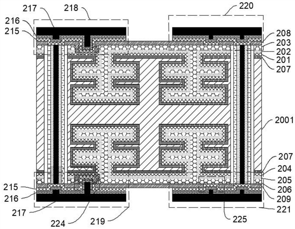
[0066]For the problems present in the prior art, embodiments of the present invention provide a three-dimensional integrated structure, specific referencefigure 1 Or 19, including: housing, the housing further comprises a first nano capacitor and a second nano capacitor disposed up and down, which is shown that the housing also has several intervals distributed first through holes 211. .
[0067]Specifically, the first nano capacitor includes a first bottom metal electrode layer 201 and a first top metal electrode layer 203, and the first nano capacitor is also provided with a first bottom connection hole 222 and a first top connection hole 223, Wherein, the first bottom connection hole 222 exposes a portion of the first bottom metal electrode layer 201, the first top connection hole 223, which shows a portion of the first top metal electrode layer 203.
[0068]The second nano capacitor includes a second bottom metal electrode layer 204 and a second top metal electrode layer 206, and the second nano capacitor further has a second bottom connection hole 224 and a second top connection hole 225, wherein said The second bottom connection hole 224 exposes a portion of the second bottom metal electrode layer 204 that exposes the second top metal electrode layer 206.
[0069]The conductive assembly can be provided to electrically connect the first bottom metal electrode layer 201 and the second bottom metal electrode layer 204 by a plurality of the first through hole 211, respectively, such that the first top metal electrode layer 203 and the The second top metal electrode layer 206 is electrically connected.
[0070]By setting the first nano capacitor and the second nano capacitor on the housing, the integrity of the structure is ensured, and the first through hole 211 is also opened on the housing, the conductive assembly is respectively The first bottom metal electrode layer 201 and the second bottom metal electrode layer 204 are electrically connected by the first through hole 211, so that the first top metal electrode layer 203 and the second top metal electrode layer are 206 is electrically connected to achieve parallel the first nano capacitor and the second nano capacitor, improve the nanocapacitance density, and the use of three-dimensional integration reduces the first nano capacitor and the second nano capacitor accounted for integrated structure. The surface area further enhances the overall performance of the nano capacitance.
[0071]Preferably, the first through hole 211 is set to two and is disposed at both sides of the first nano capacitor and the second nano capacitor, respectively. It will be appreciated that the first nano capacitor and the second nano capacitor are between two of the first through holes 211, and both ends of the first through hole 211 are close to the first bottom. The connecting hole 222 and the second bottom connection hole 224, and the other end of the first through hole 211 are adjacent to the first top connection hole 223 and the second top connection hole 225, respectively.
[0072]Through the above setting, it is convenient for the conductive assembly to electrically connect the first nano capacitor and the second nano capacitor to ensure integrated structural integrity, making the overall structure more compact.
[0073]Preferably, the conductive assembly includes a bottom connector and a top connector, wherein the bottom conductive assembly includes a first bottom connection end 218 and a second bottom connection end 219, the first bottom connection end 218 is located in the The first bottom connection hole 222 is used to electrically connect with the first bottom metal electrode layer 201, the second bottom connection end 219 is provided in the second bottom connection hole 224 for use with the second bottom. The metal electrode layer 204 is electrically coupled to achieve an electrical connection of the first bottom metal electrode layer 201 and the second bottom metal electrode layer 204.
[0074]The top connector includes a first top connection end 220 and a second top connection end 221, the first top connection end 220 is provided in the first top connection hole 223, and the first top metal electrode layer 203 The contact implementation is electrically connected, and the second top connection end 221 is provided in the second top connection hole 225, which is electrically connected to the second top metal electrode layer 206, thereby achieving the first top. The metal electrode layer 203 and the second top metal electrode layer 206.
[0075]Further preferably, a first insulating medium 202 is further included, and two first heterogeneous grooves are provided on the upper end of the housing, and the longitudinal section of the first shaped groove is "soil" shape, two of the first shaped grooves. The first bottom metal electrode layer 201, the first insulating medium 202, and the first top metal electrode layer 203 are sequentially set, thereby forming the first nanometer capacitor.
[0076]The first shaped groove is provided as a "soil" shape, which significantly increases the spatial area in the first nanometer capacitor, increasing the specific surface area of ​​the first nano capacitor, thereby increasing the capacitance density of the first nano capacitor. Further improve the performance of the nano capacitance.
[0077]Similarly, a second insulating medium 205 is also included, and the lower end of the housing is provided with two second shaped grooves, and the longitudinal section of the second shaped groove is "dry" shape, and then in the The second bottom metal electrode layer 204, the second insulating medium 205, and the second top metal electrode layer 206 are sequentially provided in the second shaped groove to form the second nano capacitor.
[0078]By providing the second shaped groove at the lower end of the housing, the longitudinal section of the second shaped groove is "dry" shape, the symmetry of the integrated structure is added, so that the product structure is more beautiful and clean, and significantly increased The spatial area of ​​the second nano capacitor increases the specific surface area of ​​the second nano capacitor, thereby increasing the capacitance density of the second nano capacitor, further improving the performance of the nano capacitance.
[0079]In another embodiment of the present invention, referencefigure 1 As shown, on the basis of the above embodiment, the first isolation medium 207 is further included, and when the housing is fabricated, the first shaped groove and the second shaped groove are arranged in the The first substrate 2001 is provided, and the first isolation medium 207 is provided in the first shaped groove and the second shaped groove, it is to be noted that the first isolation medium 207 will use the first bottom The metal electrode layer 201 is separated from the first shaped groove, and the second bottom metal electrode layer 204 is separated from the second shaped groove.
[0080]referenceFigure 19 As shown, when the housing is a combination of the second substrate 2002, the first alternating layer 2003, and the second alternating layer 2004, the second substrate 2002 is located at the first alternating layer 2003 and the first Between the alternating layer 2004, the first shaped groove is disposed in the first alternating layer 2003, and the second shaped groove is disposed in the second alternating layer 2004. It should be noted that in the present embodiment, the first alternating layer 2003 and the second alternating layer 2004 are SiO2Si3N4The laminated laminate of the material, so it is not necessary to provide the first heterogeneous groove and the second shaped groove disposed on the first alternating layer 2003 and the second alternating layer 2004. . When the housing is manufactured by the first substrate 2001, it is only necessary to process the first shaped groove and the second shaped groove on the housing, so that the first alternating layer 2003 and the The second alternating layer 2004 is described.
[0081]The above two preparation methods can meet the structure of the housing according to the actual production selection.
[0082]Preferably, the second isolation medium 208 and the third isolation medium 209 are further included, the second isolation medium 208 is provided in the first bottom connection hole 222 and the first top metal electrode layer 203 upper surface, The first top connection hole 223 is disposed at the second isolation medium 208 and is turned on to the first top metal electrode layer 203. Thereby, the first top metal electrode layer 203 and the first bottom metal electrode layer 201 are revealed in the first nano capacitor.
[0083]The third spacer medium 209 is disposed in the inner side surface of the second bottom connection hole 224 and the second top metal electrode layer 206, the second top connection hole 225 is disposed at the third isolation medium 209, and Turn on to the second top metal electrode layer 206. Thereby, the second top metal electrode layer 206 and the second bottom metal electrode layer 204 are revealed in the second nano capacitor.
[0084]The feasibility of the first nano capacitor and the second nano capacitor is achieved by the above-described structural design. At the same time, the setting of the second isolation medium 208 and the third isolation medium 209 also guarantees the reliability of the parallel structure to avoid electrical connections that may be present in the integrated structure, thereby affecting the first nano capacitance and the Parallel of the second nano capacitor.
[0085]Preferably, the bottom connector further includes a bottom connection body, the bottom connection body connects the first bottom connection end 218 and the second bottom connection end 219, the top connector further comprising top connection main body, The top connection body is connected to the first top connection end 220 and the second top connection end 221.
[0086]In this embodiment, the bottom connection body, the first bottom connection end 218, the second bottom connection end 219, the top connection body, the first top connection end 220, and the second top connection end 221, allocated in the form of a deposition process, thereby ensuring the stability and reliability of the bottom connector and the top connecting structure.
[0087]Further preferably, the bottom connection body and the top connection body each include the fourth spacer medium 210, the first diffusion barrier layer 212, the first seed layer 213, and the first metal layer 214, the bottom connection. The main body and the top connection body are provided in two of the first through holes 211, respectively, and fill two of the first through holes 211, respectively.
[0088]The integrity of the integrated structure is supported by the bottom connection body and the top connection body in two first through holes 211.
[0089]Preferably, the first bottom connection end 218, the second bottom connection end 219, the first top connection end 220, and the second top connection end 220, including the second diffusion barrier layer 215 set up in turn. The second seed layer 216 and the second metal layer 217, the second diffusion barrier layer 215, the second seed layer 216, and the second metal layer 217 form a convex portion, four of the convex portions. The first bottom connection hole 222, the second bottom connection hole 223, and the second top connection hole 225 are adapted to the first bottom connection hole 222, the second bottom connection hole 225, respectively.
[0090]By sequentially set the second diffusion barrier layer 215, the second seed layer 216 and the second metal layer 217 formed with the first bottom connection hole 222, the second bottom connection hole 224, the first top connection hole 223, and the first The two top connecting holes 225 adapt, thereby ensuring the integrity of the integrated structure.
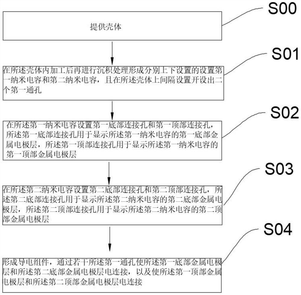
[0091]In another embodiment of the present invention, referenceFigure 2-17As shown, a three-dimensional integrated structure manufacturing method includes the following steps:
[0092]S00: Provide housing;
[0093]S01: After processing in the housing, deposition processing is performed to form a first nano capacitor and a second nano capacitor provided up and down, and a plurality of first through holes 211 are opened on the housing.
[0094]S02: The first bottom connection hole 222 and the first top connection hole 223 are provided at the first nano capacitor, and the first bottom connection hole 222 is used to display the first bottom metal electrode layer 201 of the first nano capacitor. The first top connection hole 223 is used to display a first top metal electrode layer 203 of the first nano capacitor;
[0095]S03: The second bottom connection hole 224 and the second top connection hole 225 are provided at the second nano capacitor, and the second bottom connection hole 224 is used to display the second bottom metal electrode layer 204 of the second nano capacitor. The second top connection hole 225 is configured to display a second top metal electrode layer 206 of the second nano capacitor;
[0096]S04: Forming a conductive assembly, electrically connecting the first bottom metal electrode layer and the second bottom metal electrode layer by a plurality of said first via aperture, and causes said first top metal electrode layer and said second Top metal electrode layer is electrically connected.
[0097]The first through hole 211 is also provided on the housing provided, and the first through hole 211 is also opened on the housing, the conductive assembly is respectively passed The first through hole 211 electrically connects the first bottom metal electrode layer 201 and the second bottom metal electrode layer 204, and causes the first top metal electrode layer 203 and the second top metal electrode layer 206. The first nano capacitor and the second nano capacitor are realized in parallel, and the nano capacitance density is improved. In addition, the first nano-capacitor and the second nano capacitor are integrated. The surface area of ​​the structure improves the overall performance of the nano capacitance.
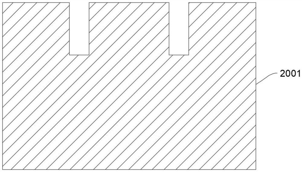
[0098]Specific, referenceimage 3 As shown in the S01, the first substrate 2001 is employed as the housing, wherein the first substrate 2001 is made of a silicon material, and the upper end of the first substrate 2001 is spinned. The top silicon blind hole is defined by exposure and development processes, and the first substrate 2001 is further etched to form the top silicon blind hole by etching the first substrate 2001 using the Deactive Ionetching, DRIE.
[0099]referenceFigure 4 As shown, the oxygen ion is then injected into the top silicon blind hole by an ion implantation manner, and the oxygen ions will diffuse down to a certain depth, and then reduce the energy of the injection of oxygen ions, and inject oxygen ions in the top silicon blind hole. At this time, the depth of oxy ion diffusion will decrease, and the energy injection of oxygen ions is continuously reduced and the foregoing injection process is repeated, thereby forming a multi-layer oxygen ion in the top silicon blind hole side wall. The first substrate 2001 is then placed in a tube furnace for annealing, and the injected oxygen ion is then reacted with the first substrate 2001 to form silicon oxide.
[0100]referenceFigure 5 As shown, by adjusting the injection energy difference between oxygen ion injection energy and the front and rear injection energy, the silicon oxide can be adjusted to the position of the top silicon blind hole side wall and the interval of the silicon oxide of the silicon oxide. Finally, hydrofluoric acid is used as an etchant to etch the silicon oxide, thereby forming two of the first shaped grooves.
[0101]Of course, nitrogen ions may be injected into the ion implantation process, thereby forming a silicon nitride material; two of the first shaped grooves are formed using hot phosphoric acid-ethaized silicon nitride.
[0102]referenceFigure 6 As shown, a layer of first isolation medium 207 is deposited inside the first shaped groove by a chemical vapor deposition method, and then the first bottom metal electrode layer is sequentially deposited on the surface of the first isolation medium 207 using an atomic layer deposition process. The first insulating medium 202 and the first top metal electrode layer 203, and the first top metal electrode layer 203 completely fills the first heterogeneous groove to constitute the first nano capacitor.
[0103]referenceFigure 7 As shown, in order to obtain a desired thickness, the structure of the lower end surface of the first substrate 2001 is removed by mechanically grinding the chemical mechanical polishing until the required thickness is obtained.
[0104]referenceFigure 8 As shown, the second shaped groove and the second nanometer capacitance structure are formed in the lower end surface of the first substrate 2001 in the same manner as in the same manner as in which the first shaped groove and the first nanome capacitance are formed. The first isolation medium 207 is deposited in advance, and then the second bottom metal electrode layer 204, the second insulating medium 205 and the second top metal electrode layer 206 are sequentially deposited, and constitute the second Nano capacitor.
[0105]referenceFigure 9 As shown, further, etching the first nano capacitor and the first substrate 2001 on the left and right sides of the second nano capacitor structure form two of the first through holes 211, and in the The first metal wiring is performed inside the first through hole 211.
[0106]Specifically, the position of the first through hole 211 is first defined by the first top metal electrode layer 203 and defines the position of the first through hole 211 by exposure and development process; followed by etching from the DRIE process. The first top metal electrode layer 203 on both sides, the first insulating medium 202, the first bottom metal electrode layer 201, the first substrate 2001, the second bottom metal electrode layer 204, The second insulating medium 205 and the second top metal electrode layer 206 are described.
[0107]referenceFigure 10 The chemical vapor deposition process is then deposited in the left and right via structures 210 in the left and right via structure; then the physical vapor deposition process is subsequently deposited in the fourth isolation medium 210, and the first diffusion barrier layer 212 and the first The seed layer 213; a further electroplating process is provided on the first seed layer 213, and the first metal layer 214 is fully filled with two of the first through holes 211.
[0108]referenceFigure 11 As shown, the first diffusion barrier layer 212, the first diffusion barrier layer 212, the first fibride layer 212, the first diffusion barrier layer 212, the first seed crystal according to the chemical mechanical polishing process. Layer 213 and the first metal layer 214, i.e., forming the bottom connection body and the top connection body.
[0109]referenceFigure 12 As shown in the S02: Specifically, the first top metal electrode layer 203 and the first insulating medium 202 are first removed by the photolithography and etching process, thereby exposing the first bottom The metal electrode layer 201 and forms the first bottom connection hole 222.
[0110]referenceFigure 13 As shown, then the chemical vapor deposition process is used to grow a layer of second isolation medium 208 cover the upper surface of the second through the second through hole structure, the surface of the first bottom connection hole 222 and the first top metal electrode layer 203. The surface is then removed from the second isolation medium 208. Thereby, the fourth isolation medium 210, the first diffusion barrier layer 212, the first seed layer 213, and the first metal layer 214, the first bottom metal electrode layer 201, and the first One metal electrode layer 203.
[0111]referenceFigure 14 As shown, then, a layer of second metal diffusion barrier layer is sequentially deposited using a physical vapor deposition process, and the second seed layer 216 covers the upper surface of the first through hole 211, the first bottom metal electrode. The surface 201 bare surface, the first top metal electrode layer 203 bare surface and the surface of the second isolation medium 208.
[0112]referenceFigure 15 As shown, the second diffusion barrier layer 215 and the second seed layer 216 of the intermediate portion are further employed by photolithography and etching processes. referenceFigure 16 As shown, the second metal layer 217 is provided on the second seed layer 216 on the left and right sides of the electroplating process to form the first bottom connection end 218 and the first top connection end 220.
[0113]referenceFigure 17 As shown in the S03, in order to lead the second bottom metal electrode layer 204 and the second top metal electrode layer 206, the second bottom connection is formed as the first nano capacitor metal wiring, and the second bottom connection is formed. The end 219 and the second top connection end 221 are not described in detail herein.
[0114]In another embodiment of the present invention, referenceFigure 18 withFigure 19 As shown, when the housing employs the combination of the second substrate 2002, the first alternating layer 2003, and the second alternating layer 2004, the first use of the chemical vapor deposition process to deposit the second substrate 2002. Instead of the layer 2003 until the layer number of the first alternating layer 2003 is obtained, it is necessary to say that the first alternating layer 2003 in the present embodiment is from SiO.2Si3N4Made of laminated, where Si3N4As a sacrificial layer. Next, the photoresist is then defined by the exposure and development process, and the first alternating layer 2003 is etched by the DRIE process until it is exposed to the second substrate. 2002 SIO2The layer, thereby forming a blind hole structure, and finally selective etching of the first alternating layer 2003 in the first alternating layer 2003 in the first alternating layer 2003.3N4Material, thereby forming the first shaped groove provided by two intervals.
[0115]Next, a layer of the first bottom metal electrode layer 201, the first insulating medium 202, and the said first insulating medium 202 and the same are sequentially deposited in the first heterogeneous groove and the first alternate groove and the first alternating layer. The first top metal electrode layer 203 forms the first nano capacitor. It should be noted that the machining process does not require depositing the first isolation medium 207 within the first shaped groove.
[0116]Similarly, the second nano capacitor is prepared by preparing the same preparation process as the first nano capacitance, and the specific preparation method is no longer specified. Finally, two of the first through holes 211, the bottom connection body, the top connection body, the first bottom connection end 218, the second bottom connection end 218, the second bottom connection end 218 The bottom connection end 219, the first top connection end 220, and the second top connection end 221.
[0117]It should be noted that the etching of the first alternating layer 2003 and the plasma of the second alternating layer 2004 can select CF4SF6CHF3CF4/ O2(CF4With O2Mixture), sf6/ O2(Sf6With O2Mixture), CHF3/ O2(CHF3With O2Any one of the mixture). And the first alternating layer 2003 and the second alternating layer 2004 can choose to select an amorphous C and Si3N4Stack, SIO2Si3N4Stack, SIO2With amorphous C stack, SIO2Geo2Stack, Si3N4Geo2Any stack of stacks.
[0118]In addition, you can choose SIO2Si3N4A material in Siion, SiCOH or SiCOFH prepares the first isolation medium 207, the second isolation medium 208, the third isolation medium 209, and the fourth isolation medium 210, can choose Tan, TiN, Any material of Wn, MON, Ni or Ru, the first bottom metal electrode layer 201, the first top metal electrode layer 203, the second bottom metal electrode layer 204, and the second top metal electrode Layer 206; selectible Al2O3Zro2, TIO2HFO2, LA2O3Any material in HFZRO, Hfalo, and HFTIO Preparation of the first insulating medium 202 and the second insulating medium 205, Tan, Tin, ZRN, MNSIO2Any of the material is prepared by the first diffusion barrier layer 212 and the second diffusion barrier layer 215, any of the materials in Cu, Ru, Co, RuCo, Curu, Cuco, prepare the first seed. The crystal layer 213 and the second seed layer 216 are greatly improved to improve the selectivity of the product material.
[0119] Although the embodiments of the present invention will be described in detail above, it will be apparent to those skilled in the art, and these embodiments can be made in various modifications and variations. However, it should be understood that such modifications and variations are within the scope and spirit of the invention described in the claims. Moreover, the invention described herein may have other embodiments, and can be implemented or implemented in a variety of ways.

PUM

no PUM

Description & Claims & Application Information

We can also present the details of the Description, Claims and Application information to help users get a comprehensive understanding of the technical details of the patent, such as background art, summary of invention, brief description of drawings, description of embodiments, and other original content. On the other hand, users can also determine the specific scope of protection of the technology through the list of claims; as well as understand the changes in the life cycle of the technology with the presentation of the patent timeline. Login to view more.

Similar technology patents

Key assembly and soybean milk machine with same

Owner:GUANGDONG MIDEA CONSUMER ELECTRICS MFG CO LTD +1

Classification and recommendation of technical efficacy words

Why Eureka
Try Eureka