
Laser driving circuit and light emitting system

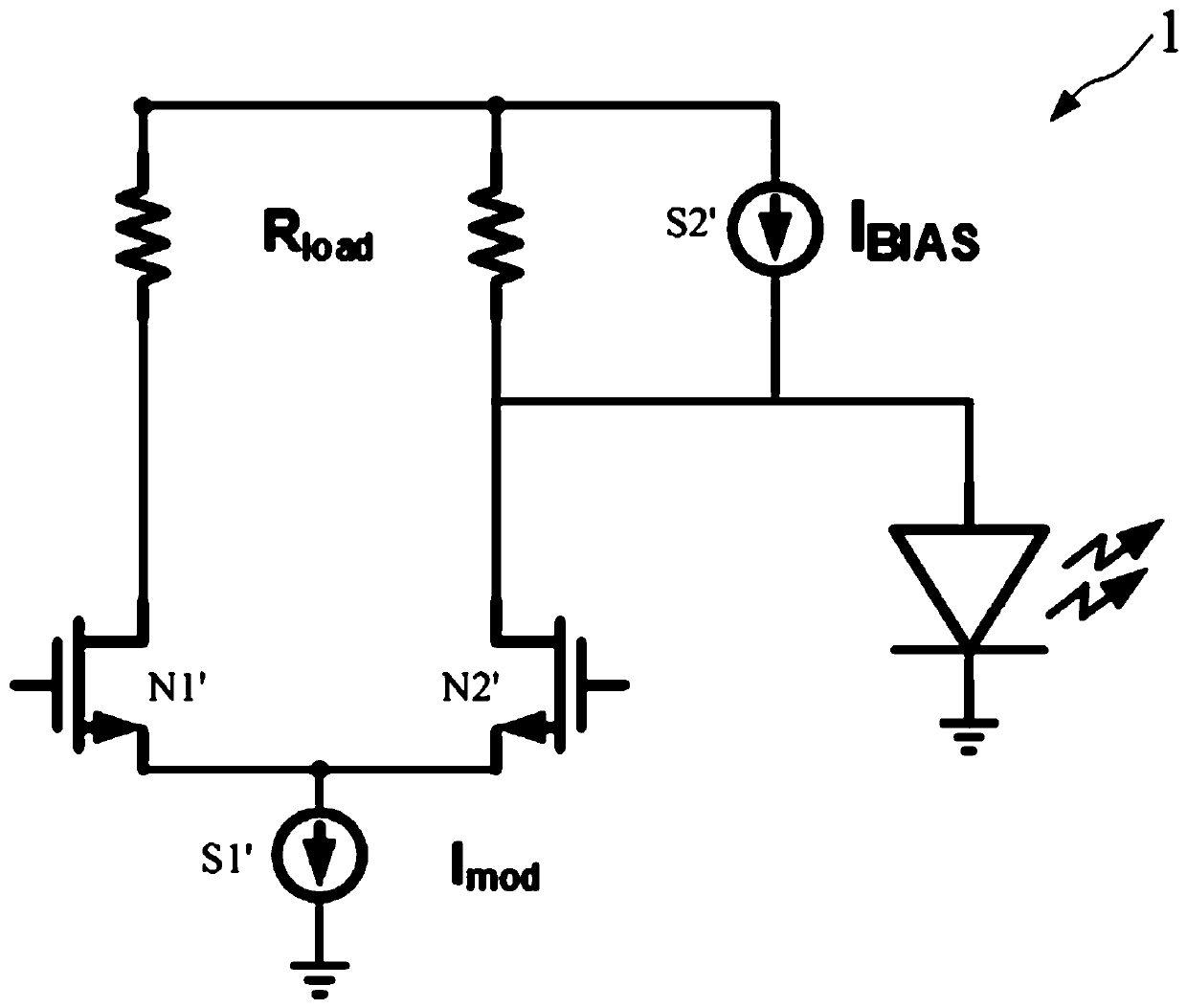
A laser drive and circuit technology, applied in the field of optical communication, can solve the problems of high power consumption and poor performance of laser drive circuits, and achieve the effect of avoiding waste of power consumption and ensuring the accuracy of bias current

Active Publication Date: 2020-06-19
PHOTONIC TECH SHANGHAI CO LTD
View PDF7 Cites 4 Cited by
  • Summary
  • Abstract
  • Description
  • Claims
  • Application Information

AI Technical Summary

Problems solved by technology

[0005] In view of the shortcomings of the prior art described above, the purpose of the present invention is to provide a laser drive circuit and a light emitting system for solving the problems of high power consumption and poor performance of the laser drive circuit in the prior art

Method used


Image

  • Laser driving circuit and light emitting system
  • Laser driving circuit and light emitting system
  • Laser driving circuit and light emitting system

Examples


Embodiment 1

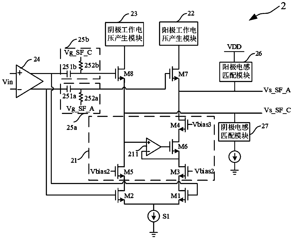
[0041] Such as figure 2 As shown, the present embodiment provides a laser driving circuit 2, and the laser driving circuit 2 includes:

[0042] Anode input transistor M1 , cathode input transistor M2 , DC operating point matching module 21 , anode load transistor M7 , cathode load transistor M8 , anode operating voltage generating module 22 and cathode operating voltage generating module 23 .

[0043] Such as figure 2 As shown, the gate terminal of the anode input transistor M1 is connected to the positive-phase input signal Vin+, the gate terminal of the cathode input transistor M2 is connected to the inversion input signal Vin-, the anode input transistor M1 and the cathode input transistor M2 After the source terminals are connected, they are grounded through the first current source S1.

[0044] Specifically, in this embodiment, the anode input transistor M1 and the cathode input transistor M2 are NMOS transistors, and the anode input transistor M1 and the cathode inpu...

Embodiment 2

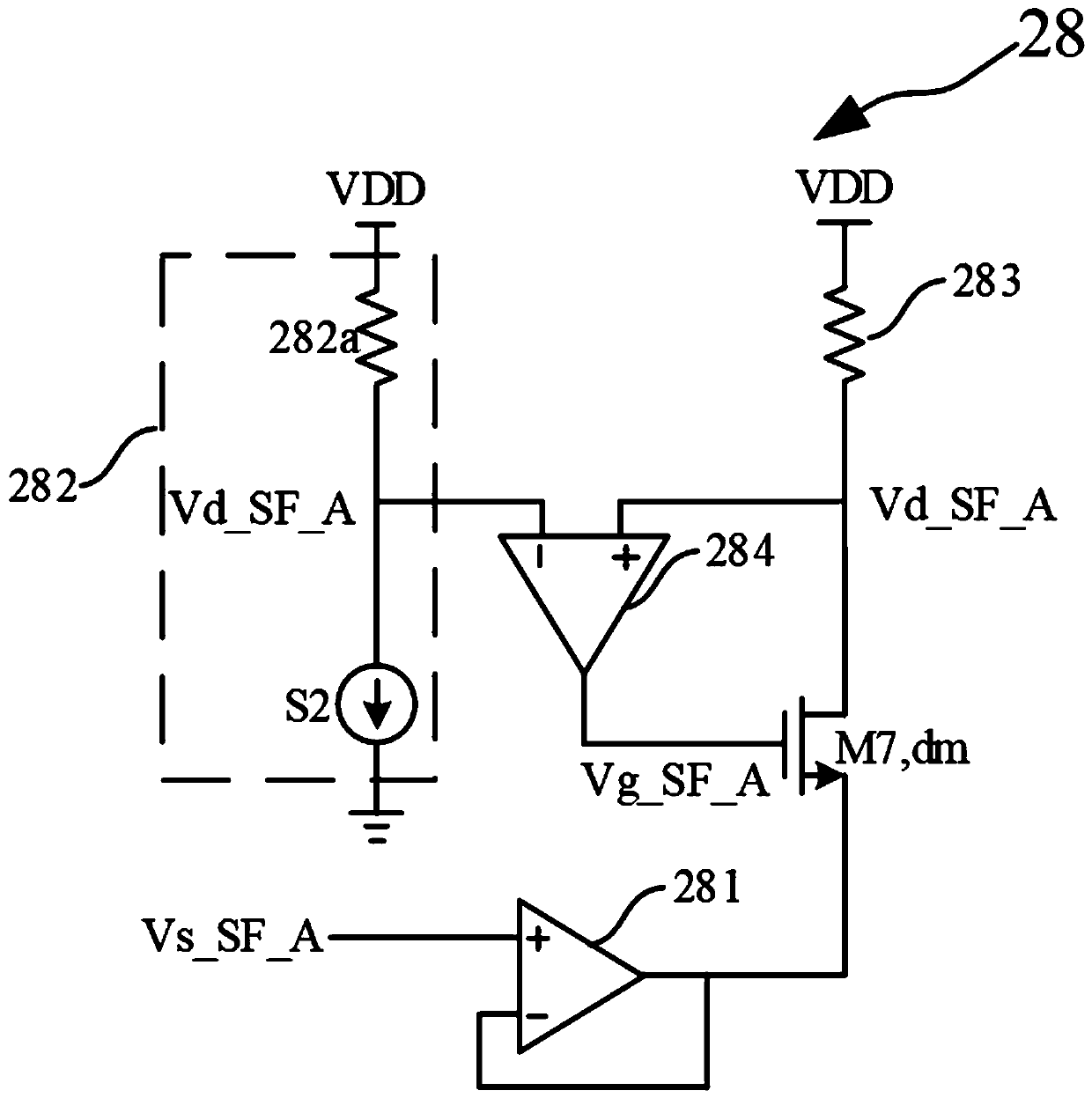
[0067] Such as figure 2As shown, this embodiment provides a laser driving circuit 2, the difference from Embodiment 1 is that the laser driving circuit 2 further includes an anode bias loop 28 for providing the anode bias signal Vg_SF_A, Such as image 3 As shown, the anode bias loop 28 adaptively generates the anode bias signal of the anode load transistor M7 based on the source terminal voltage of the anode load transistor M7 and the preset drain voltage Vd_SF_A of the anode load transistor M7 Vg_SF_A, and the preset voltage Vd_SF_A of the drain terminal of the anode load transistor M7 is used as the reference voltage of the anode working voltage generation module 22 .

[0068] Specifically, such as image 3 As shown, as an implementation of this embodiment, the anode bias loop 28 includes a first buffer 281, an anode replica transistor M7,dm, a first preset voltage generation unit 282, a first load 283 and a first One op amp 284.

[0069] More specifically, the input t...

Embodiment 3

[0077] Such as figure 2 As shown, this embodiment provides a laser driving circuit 2, the difference from Embodiment 2 is that the laser driving circuit 2 further includes a cathode bias loop 29 for providing the cathode bias signal Vg_SF_C, Such as Figure 4 As shown, the cathode bias loop 29 adaptively generates the cathode bias loop 29 based on the source terminal voltage of the cathode load transistor M8 and the difference between the drain-source voltages of the cathode load transistor M8 and the anode load transistor M7. The anode bias signal Vg_SF_C of the load transistor M8 and the preset drain voltage Vd_SF_C of the cathode load transistor M8, and the drain preset voltage Vd_SF_C of the cathode load transistor M8 is used as the reference of the cathode operating voltage generation module 23 Voltage.

[0078] Specifically, such as Figure 4 As shown, as an implementation of this embodiment, the cathode bias loop 29 includes a second buffer 291, a cathode replica tr...


PUM


Abstract

The invention provides a laser drive circuit and a light emitting system. According to the circuit, an anode input transistor and a cathode input transistor receive differential input signals, and are grounded through a first current source after the source ends are connected; a direct-current working point matching module is connected with the drain ends of the anode input transistor and the cathode input transistor and is used for matching direct-current working points, so that the currents flowing through the anode input transistor and the cathode input transistor are equal; the gate endof an anode load transistor is connected with an inverting input signal and an anode bias signal; and the gate end of a cathode load transistor is connected with a normal-phase input signal and a cathode bias signal. According to the invention, a source follower is used as an output load, so that waste of power consumption is avoided; the contradiction between low power consumption and large bandwidth is broken through; and an anode bias loop and a cathode bias loop are adopted for bias, so that direct-current working points are matched; and the precision of bias current output to a light-emitting diode is further ensured.

Description

technical field [0001] The invention relates to the field of optical communication, in particular to a laser drive circuit and an optical emission system. Background technique [0002] As data centers and high-performance supercomputing gradually use optical interconnects to replace copper interconnects to meet the increasing bandwidth requirements, whether it is directly modulated lasers or externally modulated lasers, the power consumption of the optical transmitter chip accounts for the overall power consumption of the module. A large part, so improving the energy efficiency of the optical transmitter chip is the main direction of current research and development. The laser drive circuit is the main power consumption module of the optical transmitter chip, accounting for more than 50%, so reducing the power consumption of the laser drive circuit can significantly reduce the power consumption of the overall transmitter chip. At the same time, the bandwidth is also an impo...

Claims


Application Information

Patent Timeline
IPC IPC(8): H01S5/042
CPCH01S5/042H01S5/0427
Inventor 胡上
Owner PHOTONIC TECH SHANGHAI CO LTD
Learn More