

A kind of tvs chip glass passivation screen printing screen plate and its process method
Patent Information
- Authority / Receiving Office
- CN · China
- Patent Type
- Patents(China)
- Current Assignee / Owner
- TIANJIN HUANXIN TECH DEV
- Publication Date
- 2021-05-14
Smart Images
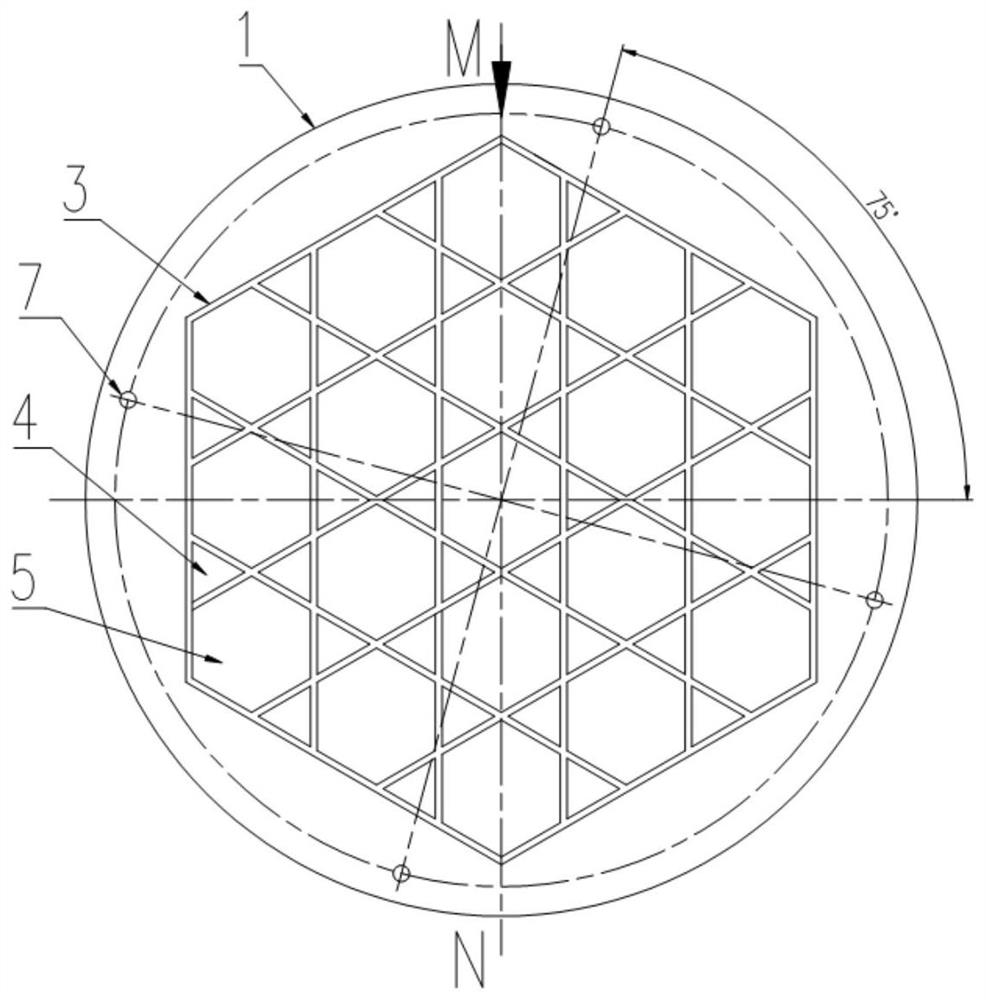
Figure 1 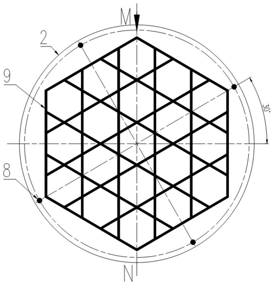
Figure 2 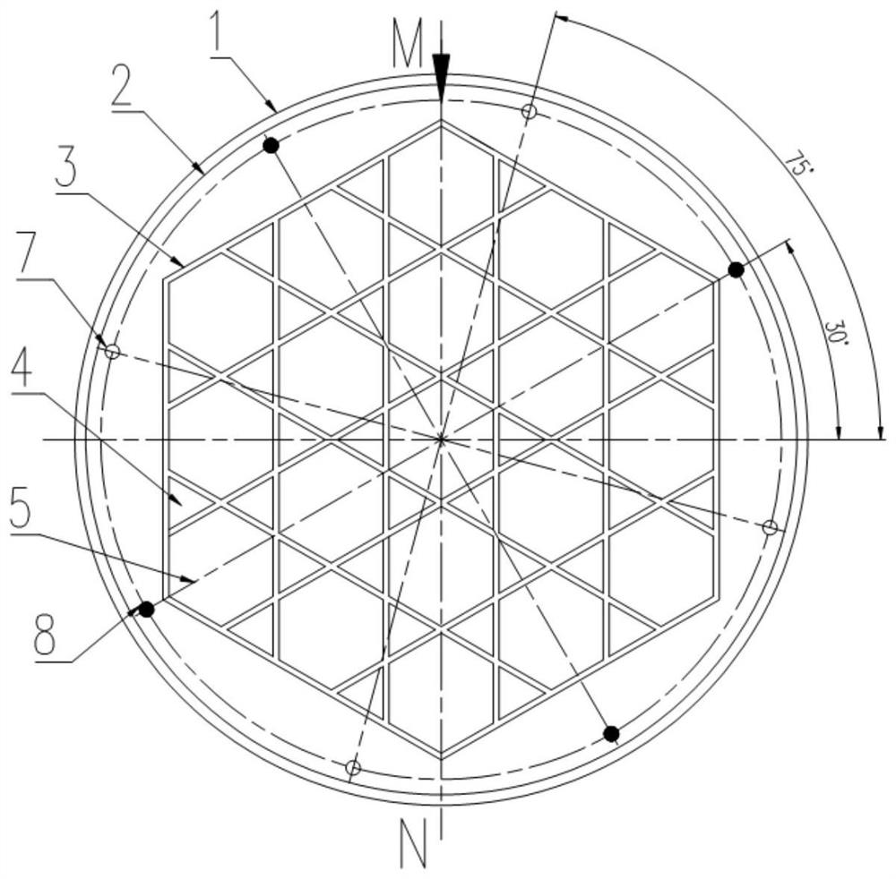
Figure 3
Abstract
Description
Technical field
[0001] The present invention belongs to the field of semiconductor devices, in particular to a TVS chip glass passivation screen printing screen and a process method thereof.Background technique
[0002] The glass passivation screen printing process has gradually replaced the previous electrophoresis, photoresistance, and blade method, widely applied to the semiconductor device printing field due to its long-scale cost, low cost, low organic solvent, and high safety factor. The glass passivation layer can not only improve the parameters of the semiconductor device, but also enhance the stability and reliability of the semiconductor device, but also provide good surface mechanical protection for the back proof process. The TVS (Transient Voltage Suppressor) chip is a highly used high-performance semiconductor circuit protection device in the current market. The printed inside of the existing scraper is cut from the edge of the TVS chip, because the TVS chip size graphic is ...