Packaging structure and packaging method of semiconductor chip

A packaging structure and packaging method technology, applied in the direction of semiconductor devices, semiconductor/solid-state device manufacturing, semiconductor/solid-state device components, etc., can solve the problem of affecting the strength and durability of the metal wire layer structure, and increase the stress concentration of the metal wire layer. , destroying the reliability of the chip packaging structure, etc., to ensure the structural strength and durability, reduce the number of inflection points, and ensure the functionality and service life.

Pending Publication Date: 2022-03-08
苏州科阳半导体有限公司
View PDF0 Cites 0 Cited by
  • Summary
  • Abstract
  • Description
  • Claims
  • Application Information

AI Technical Summary

Problems solved by technology

However, the insulation structure usually includes two layers of insulation layers, and the coverage area of ​​the two layers of insulation layers decreases from bottom to top, that is, a stepped surface is generated at the side wall of the insulation structure, so that the metal wire layer covering the side wall of the insulation structure has an inflection point, and at the inflection point Larger resistance increases the heat generation on the metal wire layer. Excessive heat reduces the reliability of destroying the chip packaging structure. It also increases the location of stress concentration on the metal wire layer and increases the possibility of metal wire layer breakage. , affecting the structural strength and durability of the metal wire layer

Method used


Image

  • Packaging structure and packaging method of semiconductor chip
  • Packaging structure and packaging method of semiconductor chip
  • Packaging structure and packaging method of semiconductor chip

Examples


Embodiment Construction

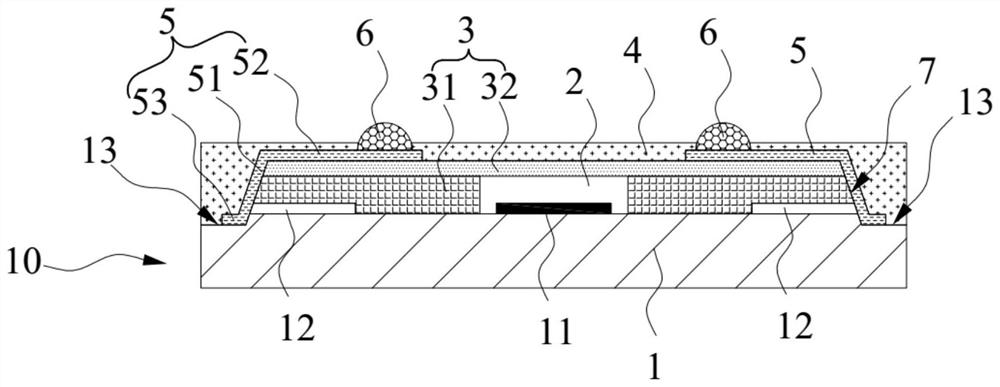
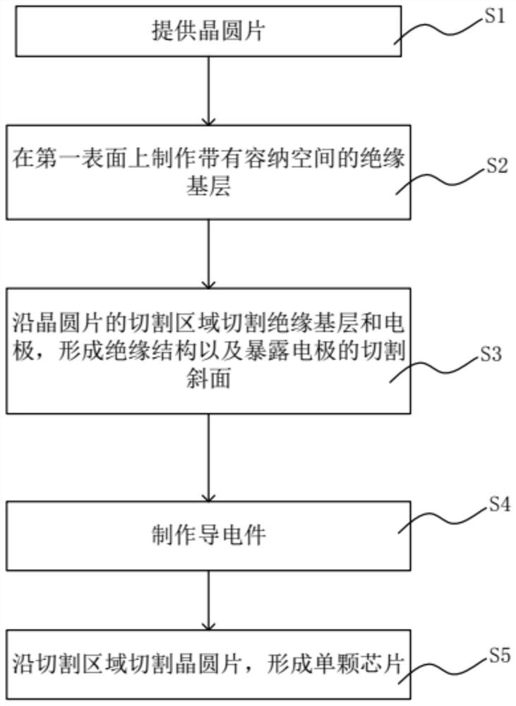
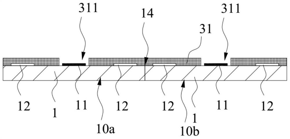
[0047]In order to make the technical problems solved by the present invention, the technical solutions adopted and the technical effects achieved clearer, the technical solutions of the embodiments of the present invention will be further described in detail below in conjunction with the accompanying drawings. Obviously, the described embodiments are only the technical solutions of the present invention. Some, but not all, embodiments. Based on the embodiments of the present invention, all other embodiments obtained by those skilled in the art without making creative efforts belong to the protection scope of the present invention.

[0048] In the description of the present invention, unless otherwise clearly specified and limited, the terms "connected", "connected" and "fixed" should be understood in a broad sense, for example, it can be a fixed connection, a detachable connection, or an integrated ; It can be a mechanical connection or an electrical connection; it can be a di...


PUM

PropertyMeasurementUnit
thicknessaaaaaaaaaa
heightaaaaaaaaaa

Abstract

The invention relates to the technical field of semiconductor packaging, and discloses a packaging structure and a packaging method of a semiconductor chip. The packaging structure of the semiconductor chip comprises a wafer, an insulation structure and a conductive part. A functional area and electrodes are arranged on the first surface of the wafer, the electrodes are distributed at intervals in the circumferential direction of the functional area, and the side walls, away from the functional area, of the electrodes are obliquely arranged; the insulating structure covers the first surface, one side of the insulating structure facing the wafer is provided with an accommodating space, the functional area is arranged between the accommodating space and the first surface, and the side wall of the insulating structure is obliquely arranged and is coplanar with the side wall of the electrode away from the functional area to form a cutting slope inclining towards the middle of the insulating structure; and the conductive part covers the cutting inclined surface and is electrically connected with the electrode, and the conductive part extends to the end surface, opposite to the wafer, of the insulating structure along the outer contour of the insulating structure. According to the invention, the conductive part is of a planar structure on the side wall of the chip, so that the number of inflection points on the conductive part is reduced, and the structural strength and durability of the conductive part are ensured.

Description

technical field [0001] The invention relates to the technical field of semiconductor packaging, in particular to a semiconductor chip packaging structure and packaging method. Background technique [0002] With the rapid development of the personal consumer electronics industry, smart devices such as notebook computers are becoming more and more portable and functional. Therefore, improving the reliability of the chip packaging structure inside the smart device is also an important development direction. In the prior art, the chip package structure includes a wafer and an insulating structure covering the wafer. In the packaging structure of one type of chip, the side wall of the insulating structure is covered with a metal wire layer, which conducts the electrical signal of the electrode on the wafer to the upper surface of the insulating structure, so as to facilitate connection with the external conductive structure. The electrodes are usually arranged at the edge of th...

Claims


Application Information

Patent Timeline
Patent Type & Authority Applications(China)
IPC IPC(8): H01L23/04H01L23/10H01L23/488H01L21/52H01L21/78
CPCH01L23/04H01L23/10H01L23/488H01L21/52H01L21/78H01L2224/11
Inventor 朱其壮倪飞龙杨佩佩金科吕军
Owner 苏州科阳半导体有限公司
Why Eureka
Try Eureka