Double-base-island heat dissipation chip packaging process

A technology of chip packaging and process, which is applied in the field of double-base island heat dissipation chip packaging process, can solve the problems of stamping deformation of lead frame blank, package deformation of lead frame blank, heat deformation of lead frame blank, etc., and achieve the effect of avoiding stamping deformation

Active Publication Date: 2020-06-23
ZHEJIANG IND POLYTECHNIC COLLEGE
View PDF5 Cites 0 Cited by
  • Summary
  • Abstract
  • Description
  • Claims
  • Application Information

AI Technical Summary

Problems solved by technology

However, as the functions of SOP products increase, the heat of SOP products also increases. In order to dissipate the heat generated inside the product as soon as possible, a groove is currently punched between the double-base islands, but the current stamping device stamps The stamping deformation of the lead frame blank located in the heat dissipation groove will occur during packaging, and the molten plastic will enter the heat dissipation groove during packaging, causing the lead frame blank around the heat dissipation groove to be heated and deformed, and then the melted plastic will flow into the lower end of the lead frame blank, causing the lead wire The package deformation of the frame blank, on the other hand, the molten plastic will enter the lower end of the lead frame blank at a certain flow rate, which will also cause the package deformation of the lead frame blank, so the packaging process needs to be improved

Method used


Image

  • Double-base-island heat dissipation chip packaging process
  • Double-base-island heat dissipation chip packaging process
  • Double-base-island heat dissipation chip packaging process

Examples


Embodiment Construction

[0024] The present invention will be further described below in conjunction with the accompanying drawings.

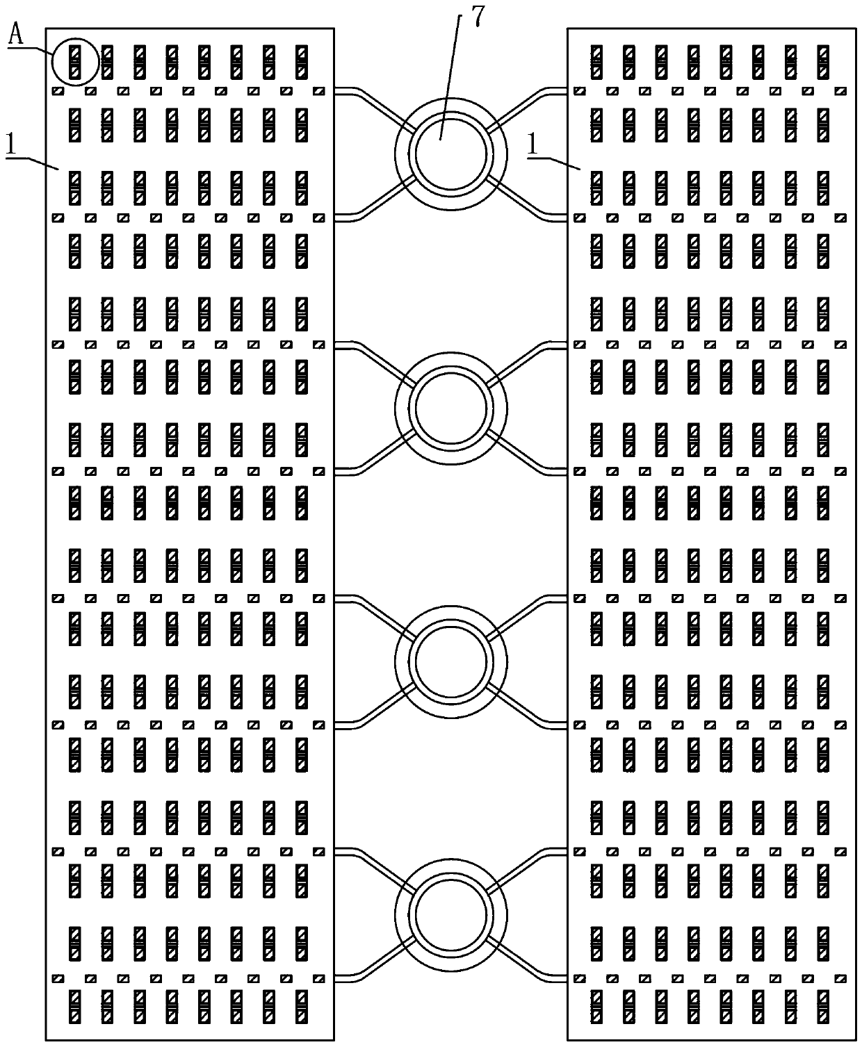
[0025] Such as Figure 1-7 As shown, a double base island cooling chip packaging process,

[0026] Step 1. Forming several base islands on the lead frame blank 1,

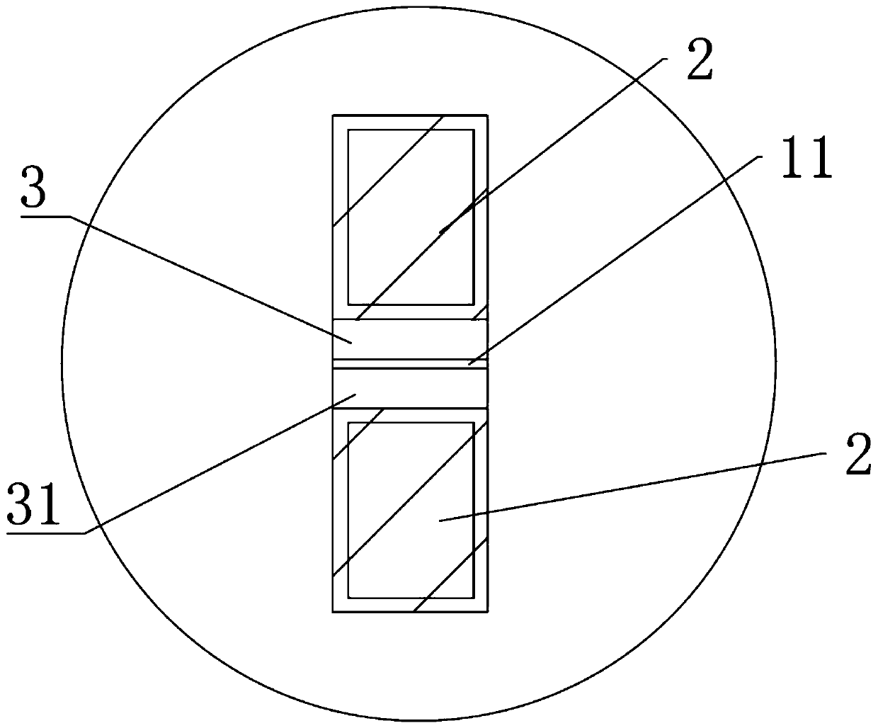
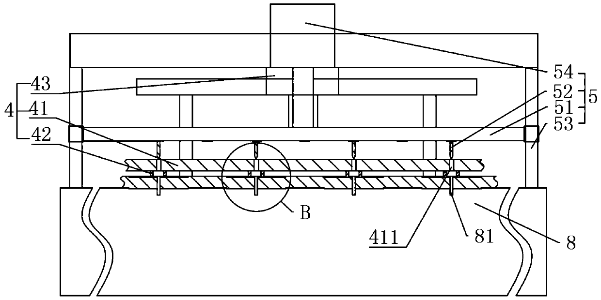
[0027] Step 2. Place the lead frame blank 1 on the stamping die base 8 of the stamping device, first press the lead frame blank 1 through the first pressing assembly 4, and the lead frame blank 1 is formed by stamping the middle part of the base island through the stamping assembly 5 The heat dissipation groove 11, the heat dissipation groove 11 runs through the upper and lower end surfaces of the lead frame blank 1, and separates the base island into a first base island 3 and a second base island 31;

[0028] Step 3. Correspondingly installing the chip 2 in the first base island 3 and the second base island 31;

[0029] Step 4. Compress the surroundings of the heat sink 11 through the second pressing co...


PUM


Abstract

The invention discloses a double-base-island heat dissipation chip packaging process. The double-base-island heat dissipation chip packaging process comprises a lead frame blank, a chip, double base islands, a stamping device and a packaging device. The lead frame blank is placed on a stamping device, the lead frame blank is pressed through a first pressing assembly, the middle of the base islandis stamped by the lead frame blank through a stamping assembly to form a heat dissipation groove, and the heat dissipation groove penetrates through the two end faces of the lead frame blank; chips are arranged at the two ends of the heat dissipation groove; the lead frame blank on which the chip is mounted is placed on a packaging device; the lead frame blank at the periphery of the heat dissipation groove is compacted through the second compaction assembly; and the upper end and the periphery of the chip are subjected to plastic package through the plastic package assembly of the packaging device, the chips at the two ends of the heat dissipation groove are subjected to plastic package to form base islands, and through the arrangement, the lead frame blank cannot be subjected to stampingdeformation during stamping and cannot be subjected to packaging deformation during plastic package.

Description

technical field [0001] The invention relates to the technical field of packaging procedures, in particular to a packaging procedure of a double-base island heat dissipation chip. Background technique [0002] Packaging (Package) is necessary and crucial for chips. Packaging can also be said to refer to the housing used to install semiconductor integrated circuit chips. It not only protects the chip and enhances thermal conductivity, but also serves as a bridge between the internal world of the chip and the external circuit. [0003] SOP (Small Outline Package) is a small outline package, which is a relatively common package form and has a wide market range. The heat generated by this package product during use can be conducted through the exposed external pins or the bottom heat sink. In order to increase the functions of SOP products, it is generally realized by multi-chip packaging, and it is common to package two chips together. When packaging an SOP chip, there are two...

Claims


Application Information

Patent Timeline
Patent Type & Authority Applications(China)
IPC IPC(8): H01L21/56H01L23/495
CPCH01L21/561H01L23/49541H01L23/49544
Inventor 徐德慧
Owner ZHEJIANG IND POLYTECHNIC COLLEGE
Why Eureka
Try Eureka