Display panel and preparation method thereof

A technology for display panels and metal layers, applied in nonlinear optics, instruments, optics, etc., to achieve the effects of reducing reflectivity, reducing color deviation, and reducing differences

Inactive Publication Date: 2020-06-26
TCL CHINA STAR OPTOELECTRONICS TECH CO LTD
View PDF5 Cites 4 Cited by
  • Summary
  • Abstract
  • Description
  • Claims
  • Application Information

AI Technical Summary

Problems solved by technology

[0003] The purpose of the present invention is to provide a display panel, which can solve the problems of adding a layer of darkening layer on the surface of the metal layer in the existing display panel, resulting in the phenomenon of strabismus, etc.

Method used


Image

  • Display panel and preparation method thereof
  • Display panel and preparation method thereof
  • Display panel and preparation method thereof

Examples


Embodiment 1

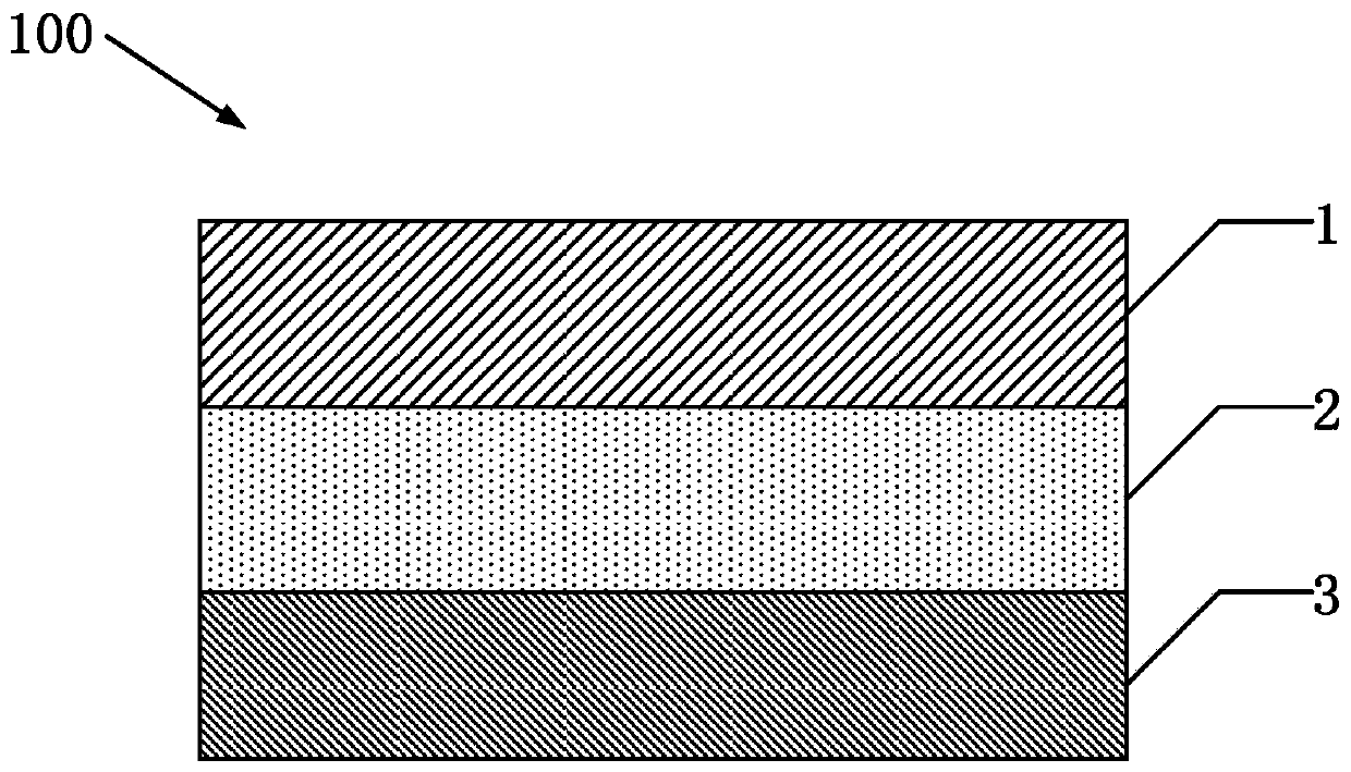
[0034] Such as figure 1 As shown, this embodiment provides a display panel 100 comprising: a metal layer 1 , a darkening layer 2 and a conductive layer 3 .

[0035] The material of the metal layer 1 includes: at least one of Cu, Mo, Ti, Al, Ni, Nb, Ta and Cr. Wherein the thickness of the metal layer is 200-700nm. Among them, 200 nm, 400 nm, and 600 nm are preferable. In this way, effects such as signal transmission can be achieved.

[0036] In fact, the display panel 100 includes a substrate and thin film transistors disposed on the substrate. The thin film transistor includes: an active layer, a gate insulating layer, a gate layer, an interlayer insulating layer, and a source-drain layer. The material of the gate layer and the source-drain layer is metal, so the metal layer 1 described in this embodiment is the gate layer and the source-drain layer in the thin film transistor.

[0037] The darkening layer 2 is disposed on one or both surfaces of the metal layer 1 , and i...

Embodiment 2

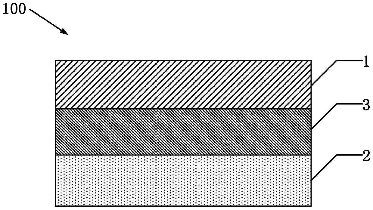
[0048] Such as figure 2 As shown, the display panel 100 of this embodiment includes: a metal layer 1 , a darkening layer 2 and a conductive layer 3 .

[0049] The material of the metal layer 1 includes: at least one of Cu, Mo, Ti, Al, Ni, Nb, Ta and Cr. Wherein the thickness of the metal layer is 200-700nm. Among them, 200 nm, 400 nm, and 600 nm are preferable. In this way, effects such as signal transmission can be achieved.

[0050] In fact, the display panel 100 includes a substrate and thin film transistors disposed on the substrate. The thin film transistor includes: an active layer, a gate insulating layer, a gate layer, an interlayer insulating layer, and a source-drain layer. The material of the gate layer and the source-drain layer is metal, so the metal layer 1 described in this embodiment is the gate layer and the source-drain layer in the thin film transistor.

[0051] The darkening layer 2 is disposed on one or both surfaces of the metal layer 1 , and in thi...


PUM

PropertyMeasurementUnit
thicknessaaaaaaaaaa
thicknessaaaaaaaaaa
thicknessaaaaaaaaaa

Abstract

The invention relates to a display panel and a preparation method thereof. A darkening layer is arranged on the surface of one side or two sides of the metal layer; a conductive layer is arranged on the surface of one side, far away from the metal layer, of the darkening layer or between the darkening layer and the metal layer. The conductive layer is used for influencing the frequency spectrum ofreflected light to reduce the difference between interference cancellation wavelengths of a front view angle and a squint angle and reduce the color deviation of the squint angle relative to the front view angle, so that the technical effects of reducing the reflectivity of the display panel and avoiding the squint angle color cast phenomenon are achieved.

Description

technical field [0001] The invention relates to the field of display technology, in particular to a display panel and a preparation method thereof. Background technique [0002] Contrast is one of the important indicators for evaluating the image quality performance of a liquid crystal display (LCD). In a real usage scenario, due to the influence of ambient light, the reflectivity of the display panel will affect the contrast of the picture. There are two ways to improve the contrast of the display panel: on the one hand, increase the brightness of the display panel in the bright state, and on the other hand, reduce the reflectivity of the display panel. The reflection of ambient light inside the display mainly comes from the reflection of metal, including the reflection of metal in the TFT area, the reflection of metal such as COM electrodes and storage capacitors. In the traditional structure, a darkening layer is added on the surface of the metal layer to absorb part of...

Claims


Application Information

Patent Timeline
Patent Type & Authority Applications(China)
IPC IPC(8): G02F1/1333G02F1/1335G02F1/1343
CPCG02F1/1333G02F1/1335G02F1/1343G02F1/13439
Inventor 于晓平林旭林
Owner TCL CHINA STAR OPTOELECTRONICS TECH CO LTD
Why Eureka
Try Eureka