
Method for producing ots device, and ots device

一种制造方法、设备的技术,应用在半导体/固态器件制造、电气元件、电固体器件等方向,能够解决困难等问题

Active Publication Date: 2020-06-30
ULVAC INC
View PDF5 Cites 0 Cited by
  • Summary
  • Abstract
  • Description
  • Claims
  • Application Information

AI Technical Summary

Problems solved by technology

That is, as a method of forming a layered body having a portion composed of a chalcogen compound and electrode portions formed above and below the portion, processing is performed in the depth direction of the layered body by one (one) etching, that is, without using Multiple gases, and it is very difficult to etch with the same gas

Method used


Image

  • Method for producing ots device, and ots device
  • Method for producing ots device, and ots device
  • Method for producing ots device, and ots device

Examples


experiment example 1

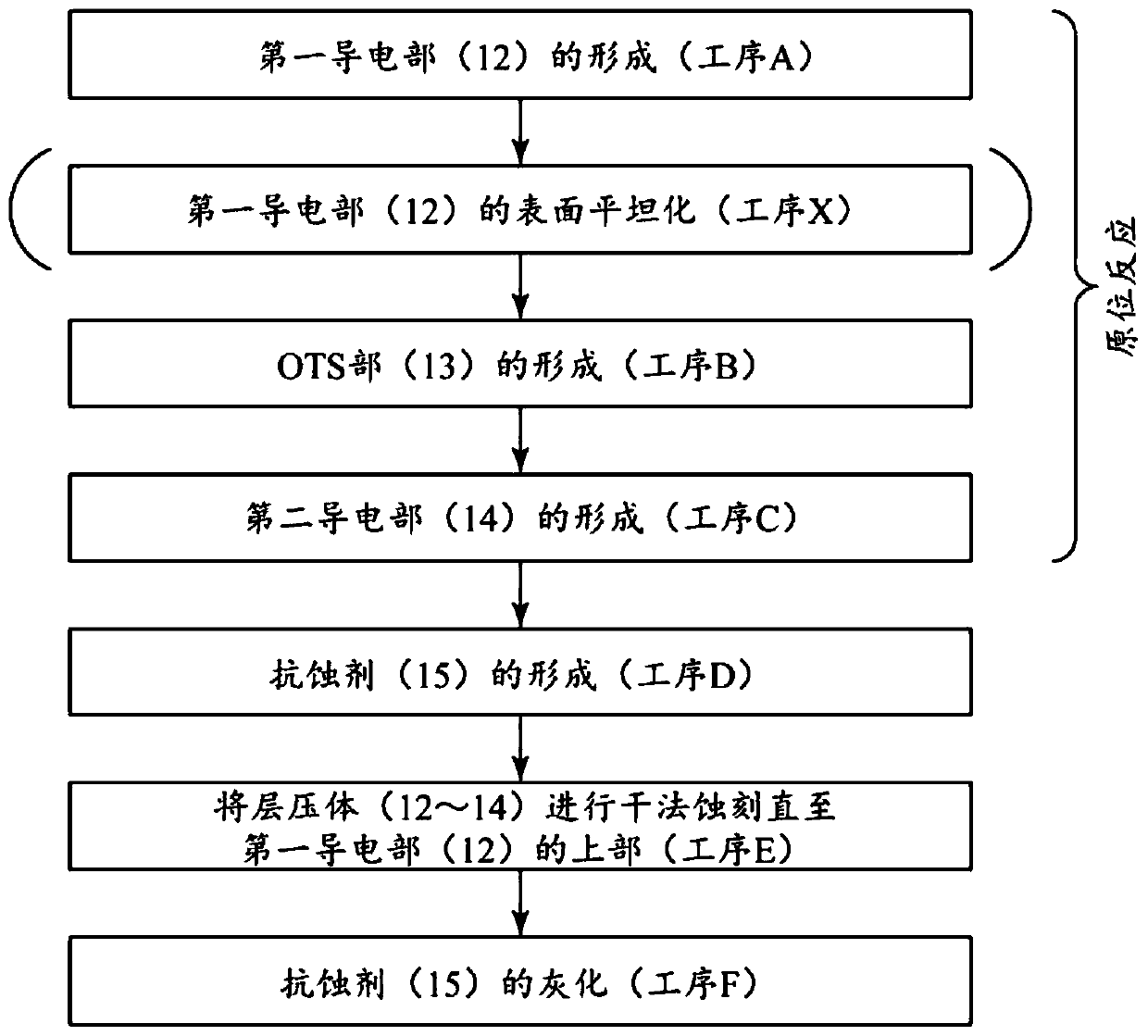
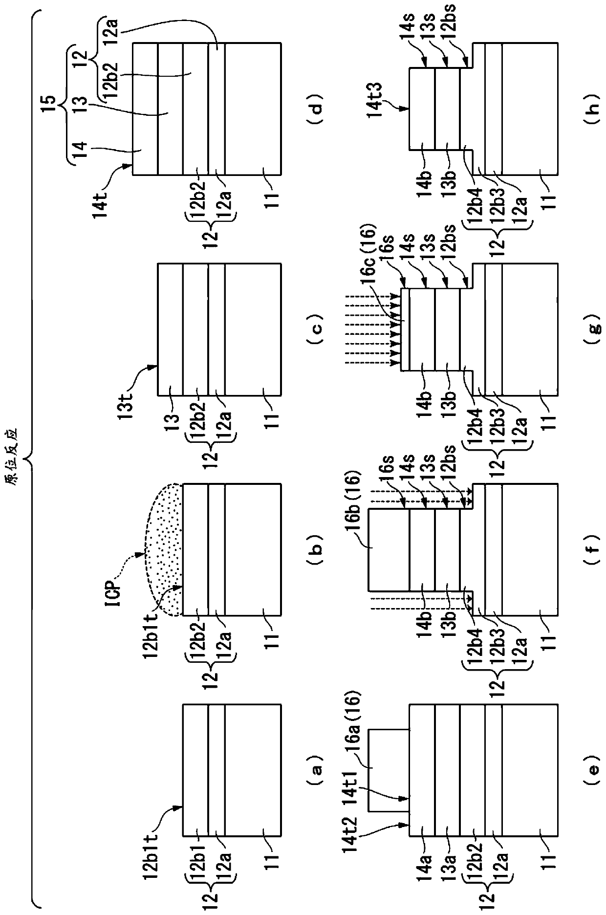
[0086] In Experimental Example 1, a series of processes consisting of the above-mentioned steps A, B, and C were all carried out under a reduced pressure atmosphere (insitu process). In the case of the second conductive portion), in step A, the first conductive portion composed of a lower layer film (Ti film) / an upper layer film (Pt film) is formed on a substrate made of Si by sputtering. Then, the surface profile of the structure formed by the in situ process was evaluated using STM (or AFM).

experiment example 2

[0088] Experimental Example 2 differs from Experimental Example 1 only in that the ICP process (process X) is performed on the surface of the first conductive part in the insitu process after the first conductive part is produced by the sputtering method in step A and before step B is performed. . Other aspects are the same as Experimental Example 1.

experiment example 3

[0090] Experimental Example 3 differs from Experimental Example 1 only in that the first conductive portion is exposed to the air before Step B is performed after the first conductive portion is formed by the sputtering method in Step A. Other aspects are the same as Experimental Example 1.

[0091] Table 1 is a list including common film formation conditions of Experimental Examples 1 to 3. Except for the TiN film, only Ar gas was used as the process gas. When it is TiN film, use Ar and N 2 formed gas mixture. Only the Ti film was formed at room temperature. All other films were formed at 150°C.

[0092] In addition, Table 1 also shows film formation conditions of a Mo film that can be used instead of TiN constituting the second conductive portion.

[0093] In Table 1, the working pressure represents the pressure at the time of film formation, the power represents the power applied to the target, the Ar gas flow rate represents the flow rate of Ar gas introduced into the...


PUM

PropertyMeasurementUnit
roughnessaaaaaaaaaa
roughnessaaaaaaaaaa
roughnessaaaaaaaaaa

Abstract

The present invention is a method for producing an OTS device in which a first conduction part, an OTS part that is formed of a chalcogenide, and a second conduction part are sequentially stacked on an insulating substrate. This production method comprises: a step A wherein the first conduction part is formed on the entire area of one surface of the substrate; a step B wherein the OTS part is formed on the entire area of the first conduction part; a step C wherein the second conduction part is formed on the entire area of the OTS part; a step D wherein a resist is formed so as to cover a partof the upper surface of the second conduction part; a step E wherein the region that is not covered by the resist is dry etched; and a step F wherein the resist is subjected to ashing. In the step E,all of the second conduction part, all of the OTS part and the upper part of the first conduction part are removed in the depth direction of the above-described region by a single etching.

Description

technical field [0001] The invention relates to a manufacturing method of an OTS device capable of realizing the stability characteristics of a two-way threshold switch (OTS: Ovonic Threshold Switch) device. Background technique [0002] As the evolution of Si-based electronic devices faces limits, innovative operating mechanisms and innovative materials are expected. Among them, chalcogenide (for example, Ge—Se, Ge—Se—Si, etc.) glass has excellent electrical characteristics, and has attracted attention as the above-mentioned material (Non-Patent Document 1). The excellent electrical characteristics are so-called characteristics of threshold switching (TS: Threshold Switch) operation. Thus, a phase-change memory (phase-change-memory) using a phenomenon of crystallization of TS, which is a diode selector device known as a nonvolatile memory device, is commercially used. [0003] Furthermore, OTS is also a promising candidate for other devices such as Metal-Oxide Silicon Fie...

Claims


Application Information

Patent Timeline
Patent Type & Authority Applications(China)
IPC IPC(8): H01L21/3065H01L21/8239H01L27/105H01L45/00H10B99/00
CPCH01L21/027H01L21/3065H01L21/321H01L21/3213H10N70/20H10N70/826H10N70/841H10N70/882H10N70/063H01L21/32115H01L21/32136H10N70/011H10N70/231H10N70/884H10B63/24
Inventor 安炯祐堀田和正沢田贵彦山本直志
Owner ULVAC INC
Learn More