Semiconductor structure and forming method thereof

A semiconductor and gate structure technology, which is applied in the field of semiconductor structure and its formation, can solve the problems of poor channel control ability of the gate structure and difficult channel, etc.

Active Publication Date: 2020-07-07
SEMICON MFG INT (SHANGHAI) CORP +1
View PDF6 Cites 0 Cited by
  • Summary
  • Abstract
  • Description
  • Claims
  • Application Information

AI Technical Summary

Problems solved by technology

However, as the channel length of the device is shortened, the distance between the source and the drain of the device is also shortened, so the ability of the gate structure to control the channel becomes worse, and the gate voltage pinches off the channel. The difficulty of the channel is also increasing, making the phenomenon of subthreshold leakage (subthreshold leakage), the so-called short-channel effect (short-channel effects, SCE) more prone to occur

Method used


Image

  • Semiconductor structure and forming method thereof
  • Semiconductor structure and forming method thereof
  • Semiconductor structure and forming method thereof

Examples


Embodiment Construction

[0031] Currently formed devices still suffer from poor performance. The reasons for the poor performance of the device are analyzed in conjunction with a method of forming a semiconductor structure.

[0032] refer to Figure 1 to Figure 5 , shows a structural schematic diagram corresponding to each step in a method for forming a semiconductor structure.

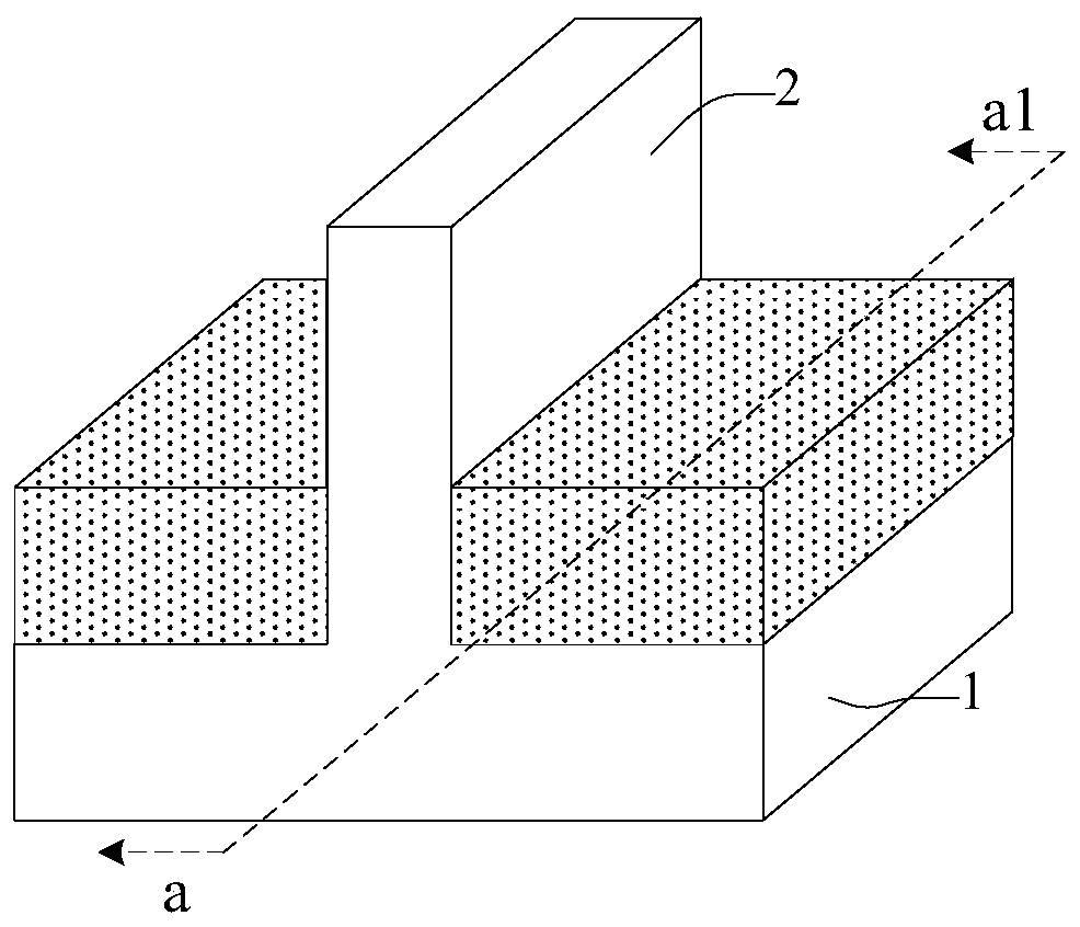
[0033] refer to figure 1 and figure 2 , showing the three-dimensional view of the semiconductor structure, figure 1 In the cross-sectional view along the aa1 direction, a base is provided, and the base includes a substrate 1 and fins 2 protruding from the substrate 1 .

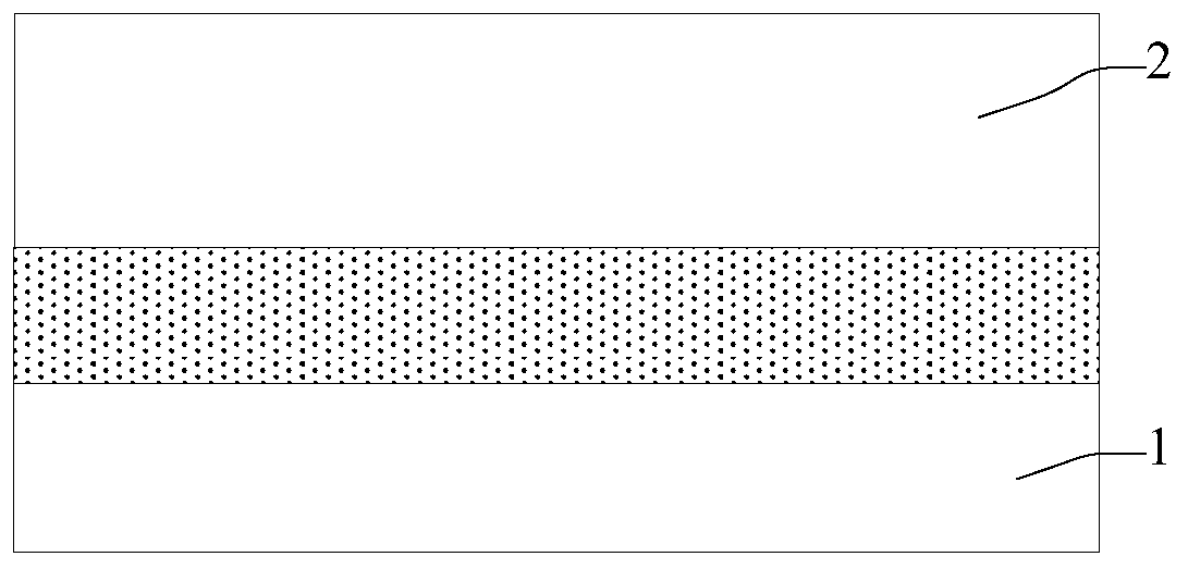
[0034] refer to image 3 , forming a gate structure material layer 3 across the fin portion 2 , and the gate structure material layer 3 covers the top and sidewalls of the fin portion 2 .

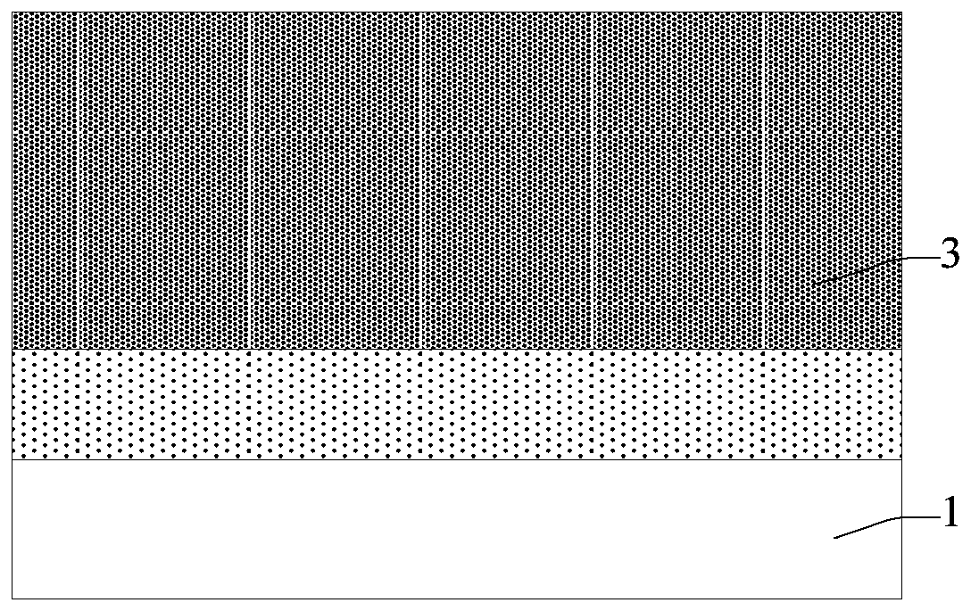
[0035] refer to Figure 4 , forming a gate mask layer 4 on the top of the gate structure material layer 3; using the gate mask layer 4 as a mask, etching the gate...


PUM

PropertyMeasurementUnit
sizeaaaaaaaaaa

Abstract

The invention provides a semiconductor structure and a forming method thereof. The forming method comprises the steps: forming a base, wherein the base comprises a substrate, a fin part protruding outof the substrate and a gate structure stretching across the fin part, the gate structure covers part of the top and part of the side wall of the fin part, and a gate mask layer is formed at the top of the gate structure; forming an isolation layer on the substrate exposed out of the fin part, wherein the isolation layer covers part of the side wall of the gate structure; after the isolation layeris formed, removing part of the width of the gate mask layer on the two sides of the gate structure, and etching the gate structure exposed by the gate mask layer by taking the residual gate mask layer as a mask and the isolation layer as an etching stop layer to form a beam-shaped gate structure, which comprises a gate structure first part located below the gate mask layer and gate structure second parts located on two sides of the gate structure first part and protruding out of the gate structure first part. According to the embodiment of the invention, the height consistency and the film quality of the second part of the gate structure can be improved, and the process difficulty of forming the beam-shaped gate structure can be reduced.

Description

technical field [0001] Embodiments of the present invention relate to the field of semiconductor manufacturing, and in particular, to a semiconductor structure and a method for forming the same. Background technique [0002] In semiconductor manufacturing, with the development trend of ultra-large-scale integrated circuits, the feature size of integrated circuits continues to decrease. In order to adapt to smaller feature sizes, metal-oxide-semiconductor field-effect transistors (Metal-Oxide-Semiconductor Field-Effect Transistor , MOSFET) channel length has been shortened accordingly. However, as the channel length of the device is shortened, the distance between the source and the drain of the device is also shortened, so the ability of the gate structure to control the channel becomes worse, and the gate voltage pinches off the channel. The channel becomes more and more difficult, making subthreshold leakage (subthreshold leakage), the so-called short-channel effect (shor...

Claims


Application Information

Patent Timeline
Patent Type & Authority Applications(China)
IPC IPC(8): H01L21/28H01L21/336H01L29/423H01L29/78
CPCH01L29/401H01L29/42356H01L29/66795H01L29/785
Inventor 张海洋纪世良
Owner SEMICON MFG INT (SHANGHAI) CORP
Why Eureka
Try Eureka