
Communication device, dielectric waveguide filter and design method thereof for suppressing far-end harmonic waves

A dielectric waveguide and filter technology, which is applied in the field of communication devices, can solve the problems of intractable harmonics in capacitive coupling, stray signals affecting the performance of communication systems, and deterioration of filter suppression effects.

Pending Publication Date: 2020-07-10
COMBA RF TECH GUANGZHOU LTD +1
View PDF0 Cites 3 Cited by
  • Summary
  • Abstract
  • Description
  • Claims
  • Application Information

AI Technical Summary

Problems solved by technology

[0003] Traditionally, the capacitive coupling method used in the design of many dielectric waveguide filters will generate far-end harmonics at the low end of the filter. However, the harmonics generated by the capacitive coupling method are difficult to deal with in the existing technology, causing the filter The suppression effect deteriorates, and good electrical performance cannot be achieved, resulting in performance indicators that cannot meet the design requirements; most of the harmonics generated by the capacitive coupling method are in the conventional communication frequency band, and spurious signals will be generated in practical applications to affect the performance of the communication system

Method used


Image

  • Communication device, dielectric waveguide filter and design method thereof for suppressing far-end harmonic waves
  • Communication device, dielectric waveguide filter and design method thereof for suppressing far-end harmonic waves
  • Communication device, dielectric waveguide filter and design method thereof for suppressing far-end harmonic waves

Examples


Embodiment Construction

[0034] In order to make the above objects, features and advantages of the present invention more comprehensible, specific implementations of the present invention will be described in detail below in conjunction with the accompanying drawings. In the following description, numerous specific details are set forth in order to provide a thorough understanding of the present invention. However, the present invention can be implemented in many other ways different from those described here, and those skilled in the art can make similar improvements without departing from the connotation of the present invention, so the present invention is not limited by the specific embodiments disclosed below.

[0035] In describing the present invention, it should be understood that the terms "center", "longitudinal", "transverse", "length", "width", "thickness", "upper", "lower", "front", " Back", "Left", "Right", "Vertical", "Horizontal", "Top", "Bottom", "Inner", "Outer", "Clockwise", "Counte...


PUM


Abstract

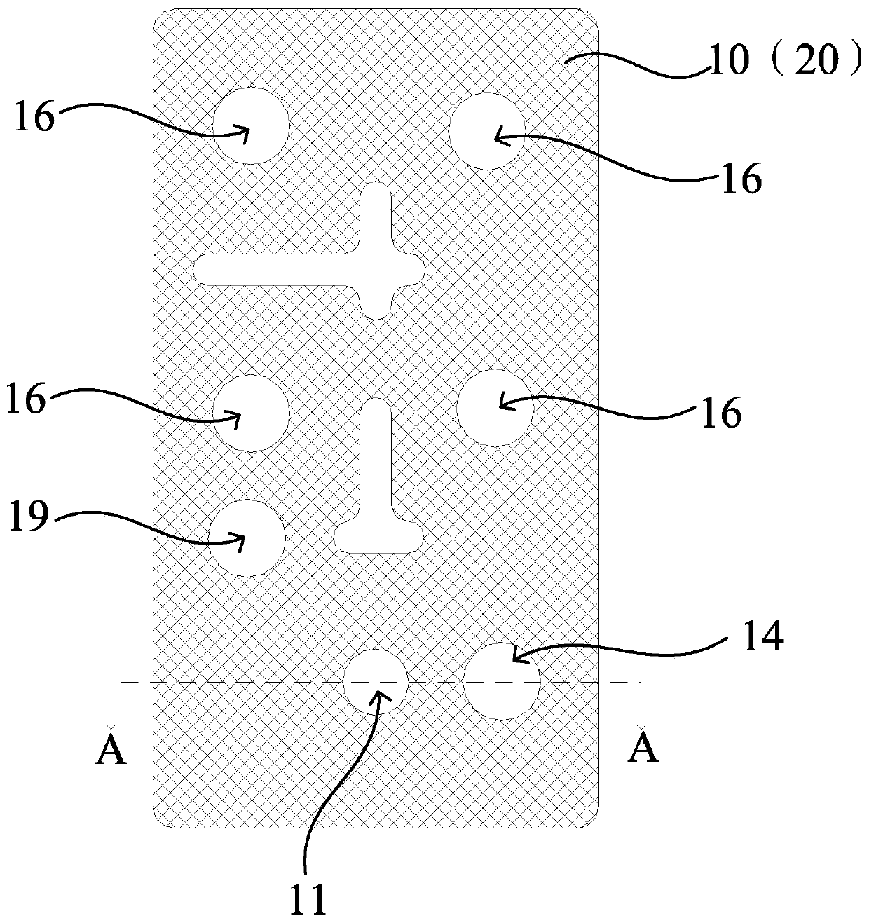
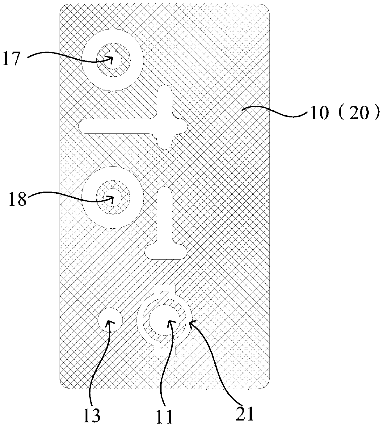
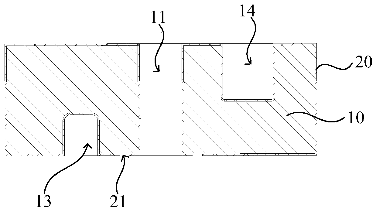
The invention relates to a communication device, a dielectric waveguide filter and a design method thereof for suppressing far-end harmonics. The dielectric waveguide filter comprises a dielectric block and a metal layer. The dielectric block is provided with a first surface and a second surface which are opposite to each other. The first surface is provided with a capacitive coupling hole, and the capacitive coupling hole extends from the first surface to the second surface. The first surface is further provided with a first frequency hole, and the first frequency hole is located on one sideof the capacitive coupling hole. The second surface is provided with a first blind hole, and the first blind hole is located on the other side of the capacitive coupling hole. The first blind hole canwell inhibit far-end harmonic waves generated by capacitive coupling, so that better electrical performance can be realized, the influence of the harmonic waves generated by capacitive coupling on acommunication system is further solved, and the filter has larger design allowance during design. Besides, the first blind hole can also be used for adjusting the capacitance coupling amount, and thedeeper the first blind hole is, the larger the capacitance coupling amount is, so that the filter is more flexible in design.

Description

technical field [0001] The invention relates to the technical field of communication devices, in particular to a communication device, a dielectric waveguide filter and a design method for suppressing remote harmonics. Background technique [0002] With the rapid development of communication systems entering the 5G era, the miniaturization of devices is the key to the development of communication equipment, and the miniaturization, high performance, and low power consumption filters are the key to the miniaturization of 5G equipment. Dielectric waveguide filters have all the characteristics of miniaturization of 5G equipment at the same time, so they have broad application prospects in 5G communication equipment. Therefore, the design method of dielectric waveguide filter has become a research hotspot. The dielectric waveguide filter improves the air filling form of the traditional waveguide filter into a high dielectric constant ceramic material filling. The ceramic dielec...

Claims


Application Information

Patent Timeline
IPC IPC(8): H01P1/20H01P11/00
CPCH01P1/2002H01P11/007
Inventor 欧阳洲黄友胜丁海
Owner COMBA RF TECH GUANGZHOU LTD
Learn More