

Array substrate and display device
A technology for array substrates and display areas, which is applied in instruments, nonlinear optics, optics, etc., can solve the problems of lower display product yield, uneven diffusion of rubbed orientation shadow liquid crystal, bright and dark areas, etc., to improve product yield and display effect, avoid the problem of uneven liquid crystal diffusion, and reduce the effect of friction weak area
- Summary
- Abstract
- Description
- Claims
- Application Information
AI Technical Summary
Problems solved by technology
Method used
Image

Examples
Embodiment Construction
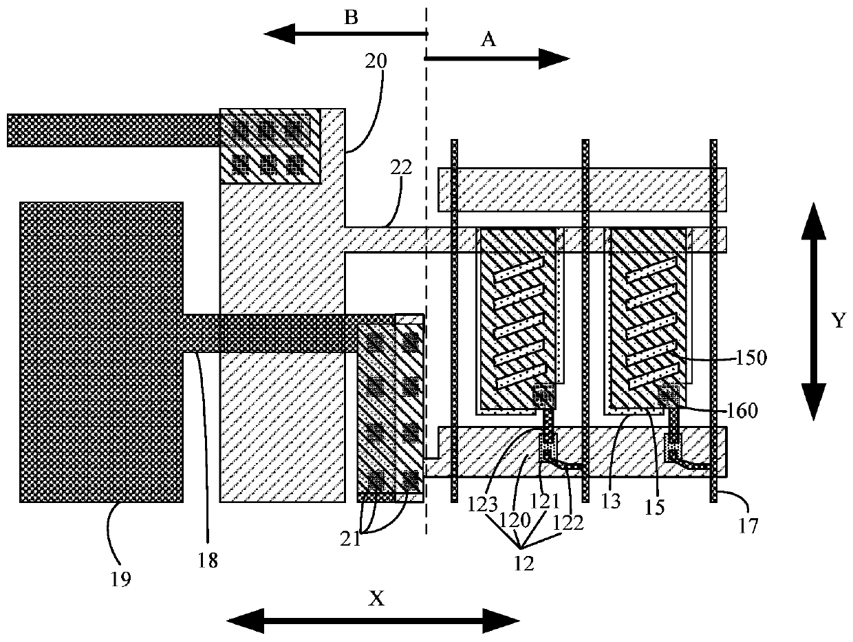
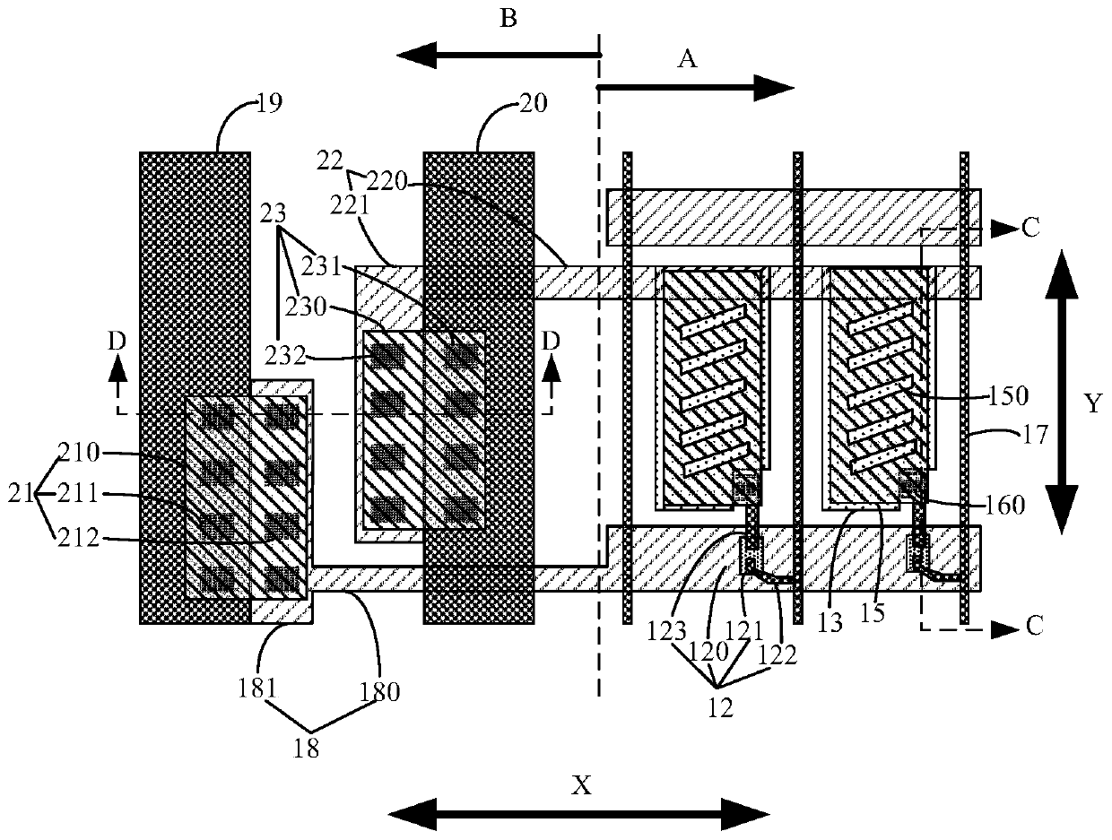
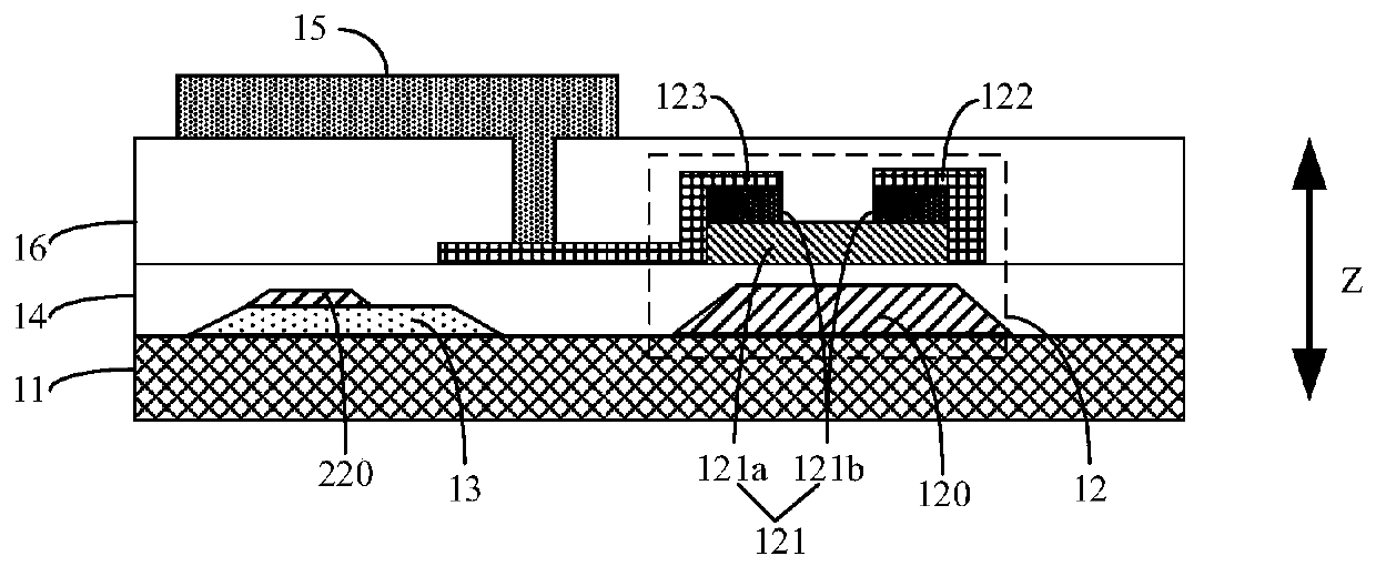
[0049] Below by embodiment, in conjunction with accompanying drawing, the technical solution of the present disclosure is described further in detail. In the specification, the same or similar reference numerals designate the same or similar components. The following description of the embodiments of the present disclosure with reference to the accompanying drawings is intended to explain the general inventive concept of the present disclosure, and should not be construed as a limitation of the present disclosure.
[0050] Additionally, in the following detailed description, for purposes of explanation, numerous specific details are set forth in order to provide a thorough understanding of the disclosed embodiments. It may be evident, however, that one or more embodiments may be practiced without these specific details.
[0051]It should be noted that "on", "formed on" and "arranged on" mentioned in this article may mean that one layer is directly formed or set on another lay...
PUM
 Abstract
Description
Claims
Application Information