Silicon wafer detecting sorting machine and sorting method thereof

A sorting machine, silicon wafer technology, applied in sorting and other directions, can solve the problems of low work efficiency, long cycle time, difficult operation, etc., to achieve the effect of fast cycle, convenient operation, and avoid hidden dangers of damage

Pending Publication Date: 2020-08-04
无锡森顿智能科技有限公司
View PDF0 Cites 7 Cited by
  • Summary
  • Abstract
  • Description
  • Claims
  • Application Information

AI Technical Summary

Problems solved by technology

[0003] The sorting of silicon wafers involves the judgment of the double-sided appearance and color of each piece. Because the silicon wafers themselves are thin and fra

Method used


Image

  • Silicon wafer detecting sorting machine and sorting method thereof
  • Silicon wafer detecting sorting machine and sorting method thereof
  • Silicon wafer detecting sorting machine and sorting method thereof

Examples


Embodiment Construction

[0045] The specific implementation manner of the present invention will be described below in conjunction with the accompanying drawings.

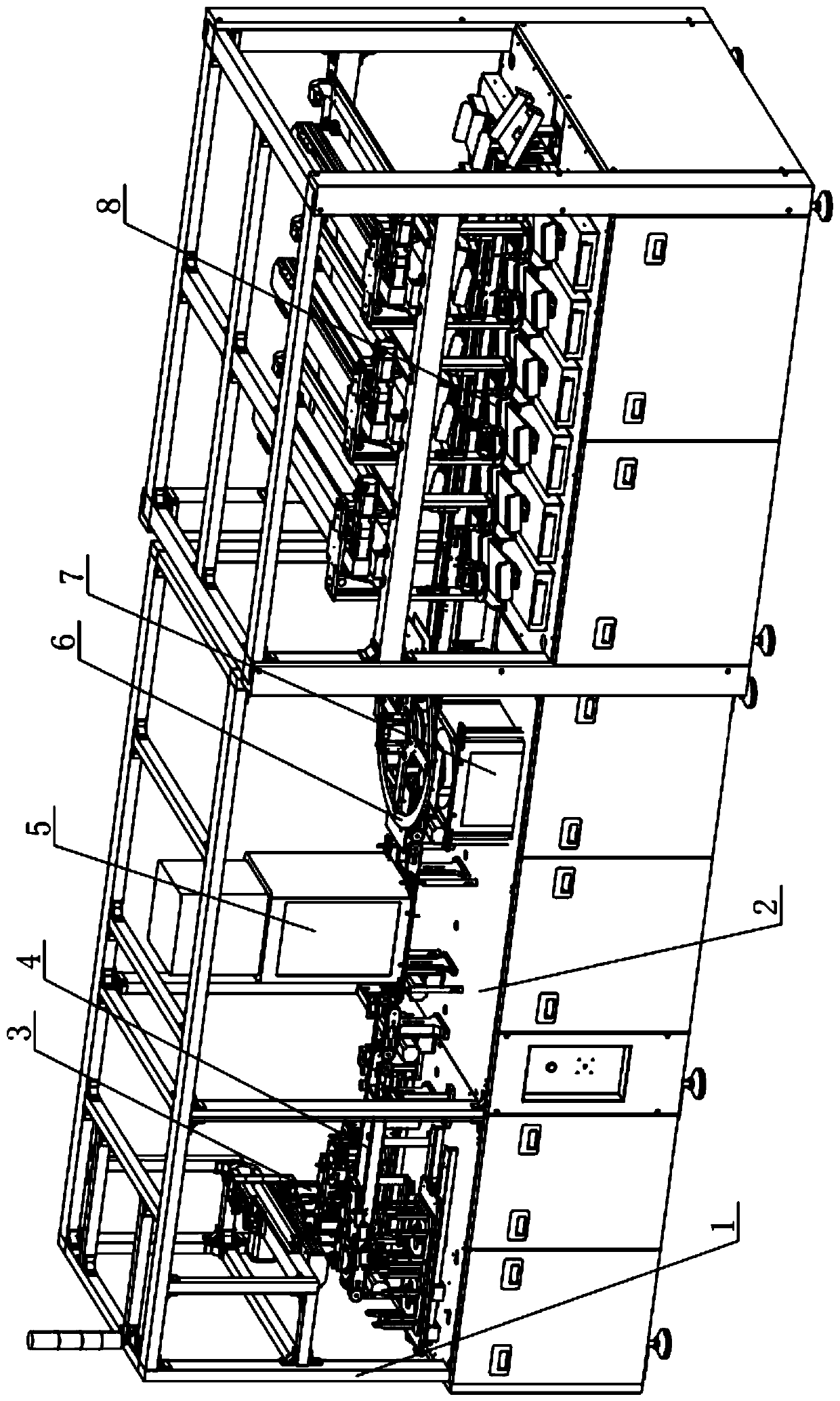
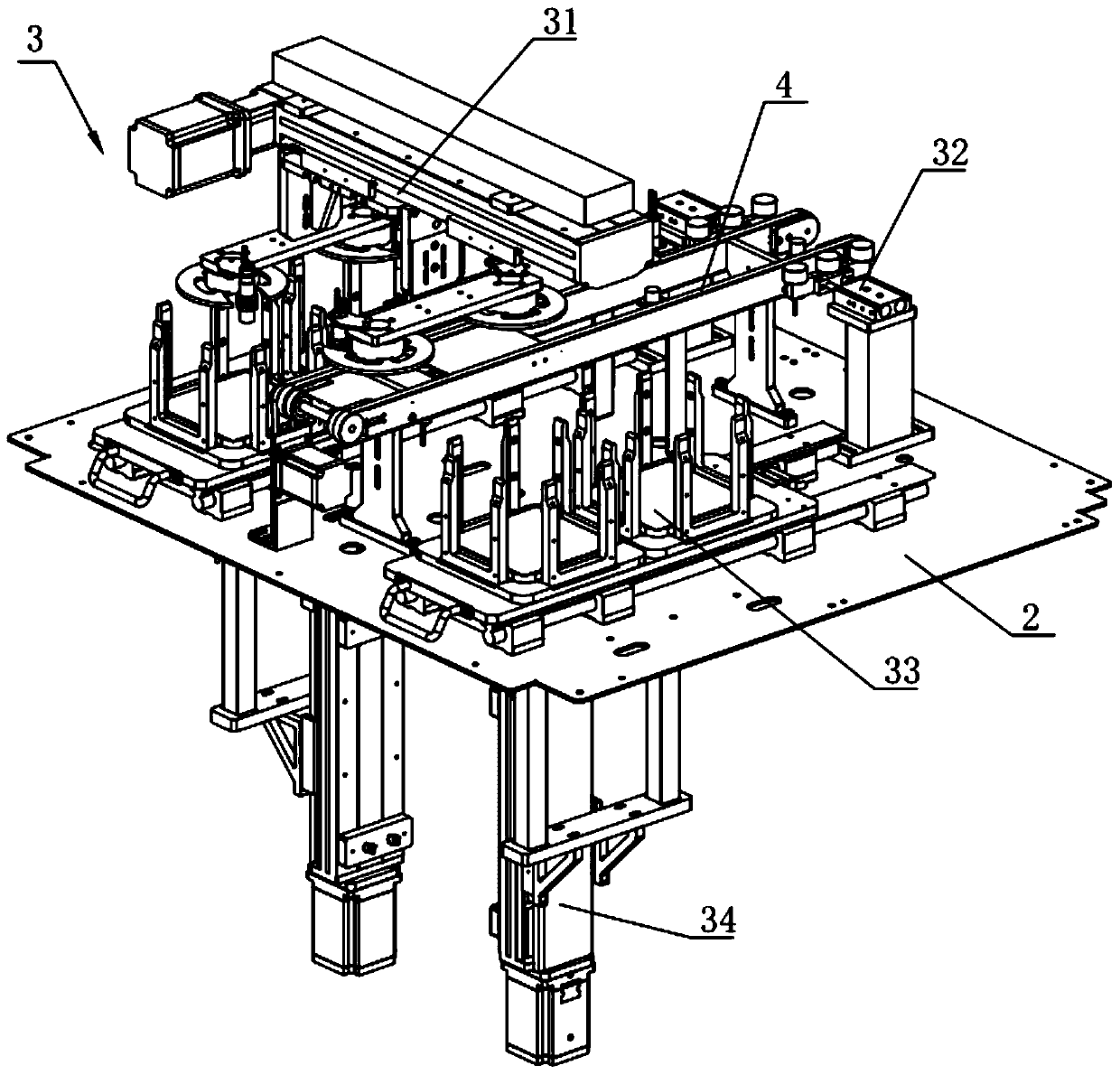
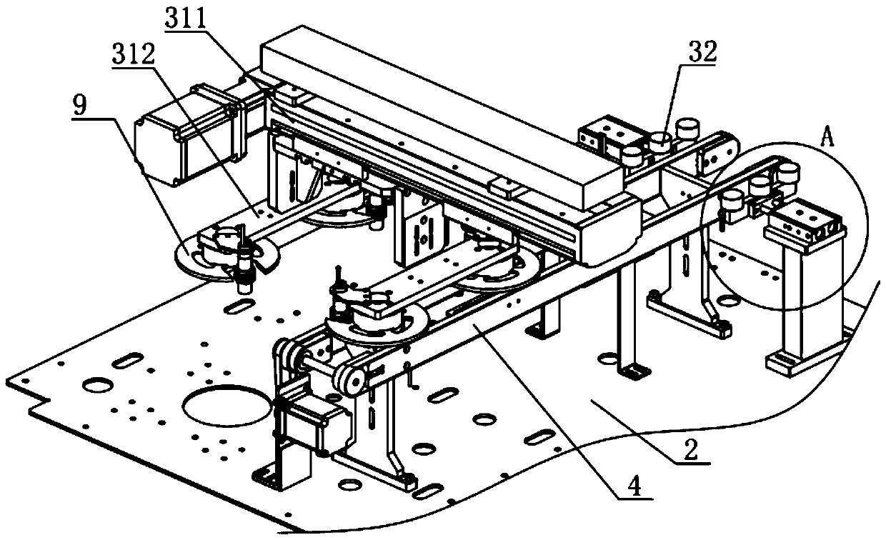
[0046] Such as figure 1 As shown, the silicon wafer detection and sorting machine of the present embodiment includes a frame 1, on which a working platform 2 is installed, and on the working platform 2, a feeding station 3, a testing station and Sorting station 8, a power conveyor belt 4 is installed in the middle of the upper surface of the working platform 2, and the power conveyor belt 4 runs through the feeding station 3, the testing station and the sorting station 8 in sequence; the testing station includes the black box one 5 and the black box two 7. Cameras are respectively installed in camera obscura 1 5 and camera obscura 2 7, one camera lens faces downward and it is located above the power conveyor belt 4, and the other camera lens faces upward and its height is lower than the height of the power conveyor belt 4.

[0047] Such a...


PUM


Abstract

The invention relates to a silicon wafer detecting sorting machine and a sorting method thereof. The machine comprises a rack, a work platform is mounted on the rack, a loading station, a detecting station and a classifying station are sequentially mounted on the work platform from left to right, a power conveying belt penetrating through the loading station, the detecting station and the classifying station in sequence is mounted in the middle of the work platform, the detecting station comprises a first camera obscura and a second camera obscura, cameras are mounted in the first camera obscura and the second camera obscura correspondingly, one camera lens faces downwards and is located above the power conveying belt, the other camera lens faces upwards, the height of the camera lens is lower than the height of the power conveying belt, a transfer mechanism moves silicon wafers to the power conveying belt from a material frame one by one, the camera in the first camera obscura carriesout front face detection, under assistance of a rotating disc mechanism, the camera in the second camera obscura carries out reverse detection, the silicon wafers with qualified appearance flow to the classifying station to be sorted to different color system material boxes along with the power conveying belt, dual-face appearance detection and color system classifying of the silicon wafers can be achieved, work efficiency is high, and silicon wafer sorting is greatly facilitated.

Description

technical field [0001] The invention relates to the technical field of photovoltaic auxiliary equipment, in particular to a silicon wafer detection and sorting machine and a sorting method thereof. Background technique [0002] With the increasing demand for high-quality solar cells in the industry, higher requirements are put forward for the quality of solar cells, including requirements for their appearance quality and color; sorted by quality and color. [0003] The sorting of silicon wafers involves the judgment of the double-sided appearance and color of each piece. Because the silicon wafers themselves are thin and fragile, it is difficult to sort and detect them. It is necessary to avoid damage to the silicon wafers. The operation is difficult and the cycle time is long. Work efficiency is low. Contents of the invention [0004] Aiming at the shortcomings of the above-mentioned existing production technology, the applicant provides a silicon wafer detection and so...

Claims


Application Information

Patent Timeline
IPC IPC(8): B07C5/00B07C5/342B07C5/02B07C5/36
CPCB07C5/00B07C5/342B07C5/02B07C5/362
Inventor 季徐华杨海波
Owner 无锡森顿智能科技有限公司
Why Eureka
Try Eureka